Charge-pump based phase-locked-loops (CPPLLs) are broadly used in various applications especially in modern communication systems [1]. CPPLLs are preferred over other topologies of phase-locked-loops (PLL) due to the advantages of large system gain, low static phase offset and low bias current. Moreover, CPPLLs ensure the stability of the PLL [2-5].
CPPLLs consist of a phase frequency detector (PFD), a charge pump (CP), a loop filter (LF), and a voltage-controlled oscillator (VCO) [6-8]. The CP is an essential component of the CPPLL, because it generates the signal and renews the clock pulses at high speeds while integrating the loop filter. In the CP, two switches process the conversion of up and down signals from the PFD into current. The PLL’s performance is determined by the PFD and CP optimized to match with zero static phase error. Numerous studies have been carried out to improve CPPLL performance within the PLL system [9-11].
The aim of this article is to study different types of CMOS CPs that have been developed for PLLs. Moreover, the relationship between the CP parameters to the quality performance of PLL is illustrated in this study. This review article is organized as follows. Section II describes the basic concepts of the conventional CP together with CP figure of merits (FOM), the various CMOS CP techniques that have been implemented in PLLs. Section III presents a performance comparison of different types of CP PLL schemes. Finally, conclusions are stated in Section IV.
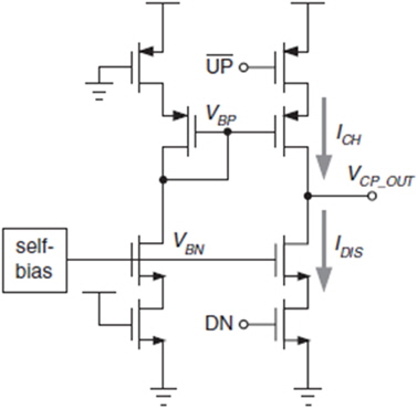
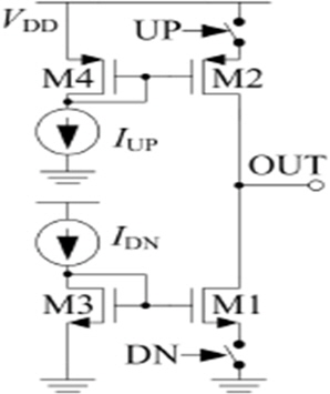
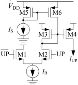
The conventional CP is single-ended, consisting of charge and discharge digital output current source, ICH and IDIS respectively as shown in Fig. 1 [12]. Two transistor switches control both digital signals, ICH and IDIS of the PFD. The two switches drive the loop filters and transfer the output signals of the PFD to analogue voltage signals, VCP_OUT, to control and charge the capacitance or frequency of the VCO [9].
Theoretically, the charge and discharge of current is equal and matched in an ideal CP, which is converted into voltage in order to tune the voltage controlled oscillator (VCO) via a loop filter [13-15]. However, realistically, the CP introduces non-idealities with static phase error instead of the expected perfect zero phase error. Thus, this non-ideal behavior creates a discrepancy between the CP and PFD, which directly leads the whole PLL system to perform sub-optimally [2,11].
To represent a measure of effectiveness, efficiency and high performance of the PLL a figure of CP merits is required. The PLL figure of merit is the normalized phase noise floor of the phase detector. A CP imperfection can be evaluated by the level of current variation, current mismatch, charge sharing, charge injection and timing mismatch. The mentioned imperfections determine the PLL’s reference spur, which is also known as dynamic jitter [7]. The amount of the reference spur, Pr is given by [9,16]:

and the loop bandwidth, fBW is given by

where, Ư is the phase error, ICP is the current flow in the CP, R is the measured value resistor in the loop filter, KVCO is the gain of VCO, N is the division value, fREF is the reference frequency for the PFD and fpl is the frequency of the pole in the loop filter. The dBc is the unit, which stands for decibel relative to carrier.
Phase error is defined as the error in significant timing and jitter source is in the PLLs using a CP. Reduction of phase error assist precisely controls the PLL dynamics [2,17]. Equation (1) shows that reference spur, Pr is proportional to the phase error, Ư and loop bandwidth (fBW). Meaning that, reference spurs can be scaled down by decreasing the phase error (Ư) by raising the reference frequency (fref) or decreasing loop bandwidth (fBW).
The high reference spur (Pr) is also attributed to the great pump current and flat current mismatch [2,9,17]. In addition, the factors of current mismatch, timing mismatch and leakage current lead the imperfection of phase error [3,8,16,18]. The mismatch and leakage current can be represented as:

where, Ư, Ưleakage, Ưmismatch and Ưtiming are the phase error, leakage current, current mismatch and timing mismatch of the CP circuit, respectively. The magnitude difference between charging and discharging currents refers to current mismatch [3,8]. In equation (3), current mismatch is directly accompanying the phase error and reference spur. Hence, a CP design is needed that is capable of minimizing the current mismatch and keeps the currents continuous across a wide output voltage range. This is the key to minimize CPPLL phase errors to create an optimum PLL system [2,11,17,19].
Other critical factors that cause current mismatch are charge injection, clock feed and current sharing. Charge injection occurs when the transistor is used to control the switching circuit. PFD output signals and the complementary signals arise when the charge leaks into a capacitive node and the mechanism is turned off [3]. In addition, when current sharing rises from the finite capacitance to the current sources, [20]. Therefore, various methods and designs to reduce current mismatch in CPs is the main target of performance improvement of the PLL, which is described in next section.
2.1 Single ended CMOS CP PLL schemes
Various single-ended CP structures have been proposed in the literature [21-24]. Single-ended CPs are popular as they do not require additional loops and can be classified into three styles according to the switch position, i.e. switch-at-drain, switch-atgate and switch-at-source [12,14,24].
2.1.1 Basic switch-at-drain and with operational amplifier (Op-Amp) CMOS CP
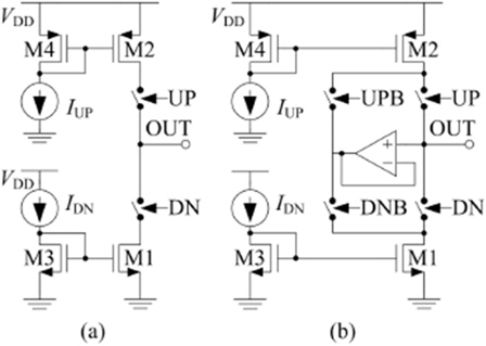
Figure 2(a) shows the fundamental switch-at-drain CP model while Fig. 2(b) provides the switch-at-drain with operational amplifier. The basic CP switch-at-drain scheme introduces two MOS switches but works sub-optimally [2,4,11]. To overcome the lack of charge sharing, an active operational amplifier was added to switch-at-drain model. With negative feedback amplification, the aim is to obtain a voltage reference equal to voltage output as long as the amplifier remains at high gain. Hence, by ensuring matched currents the voltages at both switches can be sustained [24]. The negative feedback amplifier for the CPPLL contributes to the slightly low current mismatch including a decrease in the static phase offset. However, the current mismatch still exists in the basic switch-at-drain and with op-amp CMOS CP described in this section. In addition, the feed-through of the up and down switch signals cannot be proved.
The lack of negative feedback op-amp design is due to the location of the switching transistor connected directly to the output node. Furthermore, because of the modulation effect on the channel length, mismatch between NMOS and PMOS transistors and process variations cause current mismatch [16].
2.1.2 Switch-at-gate CMOS CP
The Switch-at-Gate CMOS CP shown in Fig. 3 demonstrates how the gate is switched as an alternative to the switch-at-drain. The objective is to remove the drawbacks of the switch-at-drain. By this topology, the current mirrors result in a saturation region. The gate capacitance (MI and M2) and the long channel device are important to implement when the output current of the CP is high. To obtain better matching condition is an advantage. However, the wide and long channel device develops large parasitic capacitance, a consequence of high power consumption and low speed.
2.1.3 Basic switch-at-source and with error operational amplifier (Op-Amp) CMOS CP
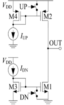
Another example of CPCLL architecture is when the switch is placed at the source of the current mirror as shown in Fig.4. This basic switch-at-source design maintains M1 and M2 in the saturation region. The switch is linked to the single transistor source with small parasitic capacitance. This topology gives the advantage of a shorter switching time compared to the gate switching design. In addition, the small bias current can be used with huge output current.
Choi,
2.2 Dual stage operational amplifier CMOS CP scheme
2.2.1 Rail-to-Rail operational amplifier CMOS CP
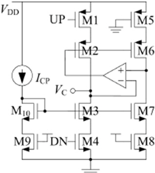
Dual stage op-amps are called rail-to-rail op-amp CMOS CP structures, consisting of negative feedback and unity gain [9,11]. As shown in Fig. 6 a rail-to-rail operational amplifier, OP1, is used. The adoption of OP1 provides a good current match within a wide output of voltage swing. The output voltage of OP1 accommodates the gate bias voltage, M5 and M6, based on the error produced between the VOUT and VF1. Thus, the values of VOUT and VF1 are perfectly matched.
In addition, the gain of OP1 must remain high. The second amplifier of unity-gain, OP2, is used to support the VOUT, VF1 and VF2 are identical. Furthermore, the designed gate lengths of all transistors are larger when compared other architecture.
2.2.2 Dual error amplifier CMOS CP
The proposed dual error amplifier CP employs a second compensation circuit or two replica-feedback amplifiers (compensator 1 and 2) with two push-pull charge pumps (CP1 and CP2) as shown in Fig. 7 [7,11]. The function of the first compensator is to control the bias voltage, VBP2, so that the charging current, ICH2, and current of the CP1 are equivalent. The second compensator also controls VBN2 to ensure the discharging current IDIS2 is equal to the charging current ICH1. This scheme’s intention is a low current mismatch.
2.2.3 Rail-to-rail operational amplifier and self-Biasing cascade CMOS CP
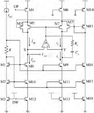
The rail-to-rail operational amplifier and self-biasing cascade, as shown in Fig. 8, is composed of a charge current switch, M4, which is located in between the VDD and M5. The discharge current switch, M12, is positioned between ground and M10. The self-biasing current mirror model comprised of the resistor cascade devices ensures that the charge and discharge currents retain an exact value [3,13,26].
On the other hand, the current of IUP is same as the current I2. The gates of M5 and M7 are biased and adjusted by the error amplifier. In this construct, the charge current, Iup, matches the discharge current, Idw. In addition, all the transistor gate lengths are also designed to be large enough.
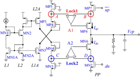
2.2.4 Dual differential amplifier CMOS CP
In the dual differential amplifier CMOS CP scheme, there are different voltage amplifiers to reduce the sensitivity of the pullup and pushdown currents. Two extra NMOSFETs as shown in Fig. 9 are added in the source branches to create the bias conditions in L1 and L2. Thus, the drain-to-source voltage drop, VDS, is matched with MP2, and MN2A. This includes MN3, which has similar voltages to VDS.
In this scheme, the voltages at nodes B and D are forced to follow nodes A and C, respectively. The area of the gain boosting CP is small compared to passive elements, making it efficient, especially for the capacitors [27].
2.3 Other CMOS charge pump schemes
2.3.1 Differential CMOS CP scheme
Differential CPs have several advantages compared to singleended ones. They are preferred to single-ended CPs in high-performance applications due to their immunity to common-mode noise and power supply variation [18,28]. Differential CPs are composed of two loop filters and a common-mode feedback circuit, as shown in Fig.10. Hence, its structure requires a large area to create extra power dissipation.
The differential amplifier is built of two current sources (NMOS and PMOS) and four switches [18,29]. In this architecture, the output of the transmission gate is connected to the loop filter. This is in addition switches the CP output current.
The two extra switches, which are toggled by the inverters (INV1 and INV2), provide a dual current flow path. When both the signals are in a high state, the current flow through transistors MP20 and MN22 move up and down. However, when both signals are in the low state, the current flows via MP17 and MN19 transistors. An amplifier of A1 is included in this structure to eliminate the impact of parasitic switches capacitance.
2.3.2 Three Rail-to-Rail Operational Amplifier CMOS CP
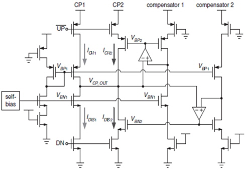
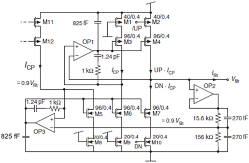
A three rail-to-rail operational amplifier often known as a compensated CP for PLL is presented in Fig. 11 [19]. The CP uses two regulation loops. One is the current source consisting of M3 and M4, the other focuses on current sink, consisting of M5, M6 and M7. The amplifier of OP1, applied in dual stage op-amp, which is included in this three rail-to-rail operational amplifier design [9]. This is due to transistor mismatch to compensate by equalizing the drain with the output of the switched current by controlling the current mirror gate bias.
However, this architecture develops new mismatch source, which is the difference between the drain potentials and the input branch. Hence, amplifier OP3 is used to match all the expected possibility. Amplifier OP2 will buffer the output voltage of the CP. This design will also regulate both source and sink currents of the CP; therefore, the need of the output potential absolute current parameter will reduce.
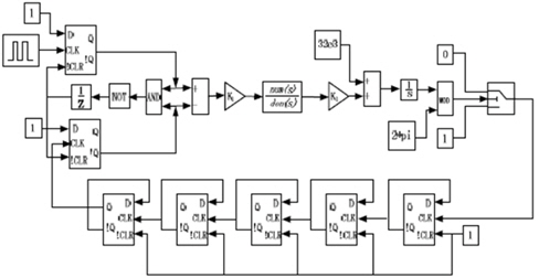
2.3.3 D-flip-flop CMOS CP
In this structure, D flip-flop CMOS CP is comprised of two D flip-flops, reset, AND gate, NOT gate, and a delay cell. After passing via the unit of NOT gate block and delay, two output signals of D flip-flop will rebound by re-setting the end of the D flip-flop [20].
The D flip-flop CMOS CP circuit is made up of transistors as shown in Fig. 12 form the current mirror in order to obtain a charging and discharging current for the low pass filter. In addition, the transistor also builds the switching circuit to adjust the output and complementary signals. The four groups of switches manage to reduce the charge injection and clock feed through. The single amplifier protects the voltage at node A and B causing them to be constantly equal with the output voltage. This is to ensure and to avoid voltage bouncing due to charge sharing
2.3.4 New source-switching CP with op-amp and current reference
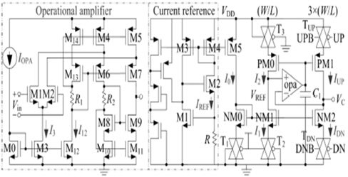
Source-switching CP with op-amp and current reference was proposed by Zhou and Wang [28]. The architecture presents the charge current, IUP and the discharge current, IDN. Both the IUP and IDN develop via the current mirrors from the same reference current source of 200 μA. In addition, a high-gain operational amplifier, as shown in Fig. 13, is also included in the CP to ensure the voltage VREF is perfectly matched to the voltage VC. However, the matching is only achievable if the gain of amplifier is maintained properly.
This design is composed with typical supply-independent current reference to provide current bias in the whole CP system. In addition, the current reference, IREF, uses only 50 μA to recover and save power consumption in the CP
The proposed design is comprised of an amplifier but has small voltage gain, relatively corresponding to 76 dB. Thus, due to the small voltage gain, the current mirror effect can be ignored and perfect current matching obtained.
2.3.5 Gain boosting charge pump for PLL
Li,
The trans-conductance and output resistance of the nMOS and pMOS are different. The enhancement of the output resistance of the two transistors in cannot be equal; this can result in current mismatch. Therefore, both up and down currents of these circuits are designed identically.
2.3.6 Operational trans-conductance amplifier CMOS CP
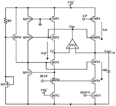
The operational trans-conductance amplifier (OTA) CMOS CP consists of a MN3 transistor, which carries low threshold voltages. The OTA is located in a feedback loop. The functions of the VOUT, Vf and Vbp nodes are to change Vbp in opposite direction. This to ensure that Vf is equal to VOUT in order to maintain OTA for a high gain.
The proposed OTA CMOS CP, shown in Fig. 15, fulfills the goal of the charge and discharge current perfectly matching. This scheme resolves current mismatch, less than 0.5% within the output voltage dynamic range from 0.2 V to 1.7 V. This includes the current variation reduced to 0.8% over the output voltage dynamic range from 0.32 V to 1.7 V.
However, the current in this design, ICH and Idis, extremely rely on output voltage variation, which is not affected the stability of the CPPLL transient response [30]. In order to reduce current mismatch and current variation, the output voltage dynamic range and power consumption are necessary to take into account.
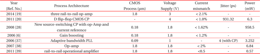
In this review, the performance of the single-ended CMOS CP for PLL can be evaluated by measuring current mismatch, current variation, reference spur and power consumption. Singleended CPs is well known, as this model does not require an extra loop filter and it offers tri-state operation with low-power consumption. In addition, single-ended CPs are divided into several types, based on the location of the switches. The basic and conventional architecture of the switch-at-drain model is suboptimal concerning current matching. Thus, the development of switch-at-drain with feedback op-amp is proposed to cater the lack of characteristics.
Switch-at-drain with feedback op-amp provides the advantage to overcome charge-sharing effects. However, the design offers extra complexity, which leads to high power consumption as measured in Table 1 [23].
[Table 1.] Performance comparison of various single-ended CMOS CP schemes for PLL.
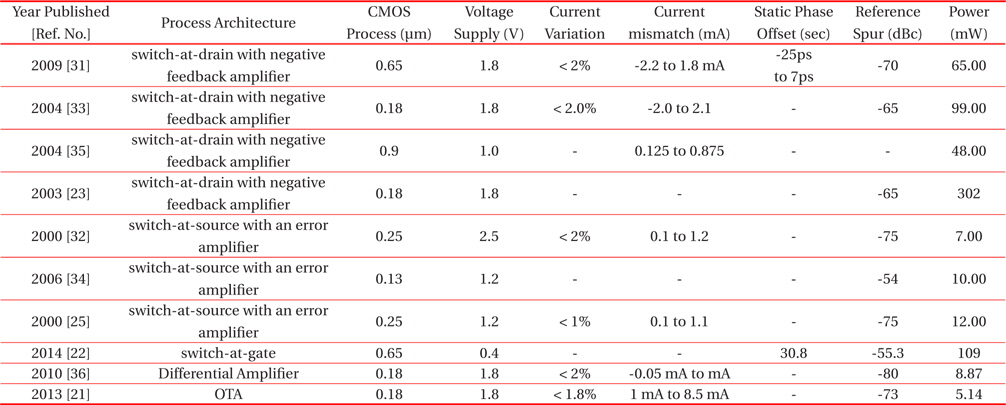
Performance comparison of various single-ended CMOS CP schemes for PLL.
The parameters for the switch-at-drain with feedback op-amp show the current mismatch is slightly reduced compared to conventional CPs. However, the measured recorded reading suggests current variation is present, due to negative op-amp feedback. Moreover, this scheme also suffers of charge injection and clock feed through.
For switch-at-gate, CMOS CP is designed to manage the drawbacks of the switch-at-drain CP presented in Moon
The switch is composed at the source of the current mirror for basic switch-at-source type. Because the switches location is not directly connected to the output, the switch errors are decreased. In addition, this architecture demonstrates shorter switching time compared to the switch-at-gate design.
The switch connection to the single source transistor gives the advantage of low parasitic capacitance. However, this design still demonstrates disadvantages with serious current mismatch, due to the finite output impedance of the current source. However, the reference current source provides low power consumption in operation compared to the rest of the architecture.
All the single-ended schemes that have been discussed can be used in CPPLLs depending on the CPPLL applications. The performances of various single-ended CMOS CP schemes for PLLs are compared in Table 1.
On the other hand, the rail-to-rail operational amplifier CMOS CP structure shows the reduction of current mismatch along with current variation. The design consists of a negative feedback amplifier, OP1 control the voltage node with high amplifier gain and give benefits of wide input voltage of charge and discharge currents. In this way, it reduces the problem of current mismatch.
In addition, larger sizes of transistor prevent the effect of channel-length modulation. OP2 is a unity-gain amplifier included in CP architecture to support and make sure the VOUT, VF1 and VF2 identical. This omits the current sharing problem. A dual error amplifier CP with two replica-feedback amplifiers, also known as unity gain op-amp. This uncomplicated, effective circuit technique and short channel circuit clear the concern of current mismatch. By reducing current mismatch and variation, the distortion can be significantly reduced. This lowers the static phase offset and spur in the PLL. The construction of dual unity gain op-amp is suitable for low voltage PLLs.
The techniques negative feedback and dual negative feedback op-amp is proposed to manage and to reduce the current mismatch significantly and align with wide current variation, but increase circuit complexity [9,11] . The constructions of larger transistors lead to a fast switching operation that allows disadvantages.
Expanding the input of rail-to-rail operational amplifier and the self-biasing cascade current mirror method enable the current of CP circuit, which is matched in a large range output voltage. Additionally, a proposed method of adding a pre-charging current source to raise the initial charge current and enhance the speed up of the CPPLL settling time. Extra consideration and stable analysis should apply to this connection as the composition simultaneously delivers a positive and negative feedback loop. In addition, the implementation of cascade current mirrors tends to reduce the voltage headroom.
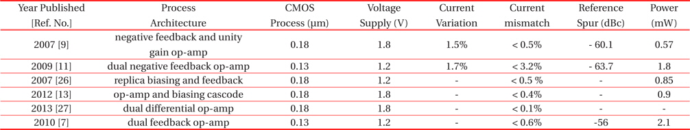
The design of dual differential amplifiers based on a switches-in-source construction improved through gain-boosting amplifiers for CPPLLs. Two differential amplifiers were employed in dual differential amplifier CPs to reduce the channel length modulation effect in MOS transistors. This is an advantage to the current up and down more towards independent of the output voltage. Nevertheless, the design is only verified by simulations. Table 2 shows the performance comparison among various schemes of dual stage op-amp CMOS CP.
[Table 2.] Performance comparison among various schemes of dual stage op-amp CMOS CP.

Performance comparison among various schemes of dual stage op-amp CMOS CP.
In addition, the method of dual stage op-amps in three rail-to-rail amplifiers is capable and proven to match the drain with the output of the switched current by adjusting the current mirror gate bias. This significantly reduces the current mismatch. However, the major concern in this design is the strength of control loops. This concern was investigated and analyses only involve in simulation. The simulation suggests a design using shortchannel devices with high voltage supply.
The design of the D flip-flop CMOS CP provides the advantages of low-power, low-jitter and high speed. The mixed architecture of digital and analog techniques contributes high precision and strength, including a high performance amplifier for CPPLLs. The D-flip-flops are included in this structure to defeat the dead phase-zone and current mirrors. The major aim of the D flip-flop CMOS CP development is to apply it in the high certainty of inertial sensors.
The gain-boosting circuit improves current matching characteristics together with the reduction of the channel-length modulationeffect. Advantages of this gain boosting CP are current mismatching characteristics are achieved without the need of stacking extra cascade devices, operational amplifiers, a feedback circuit, a complicated replica CP, and an additional compensation CP. In addition, the gain-boosting CP circuit is suitable for a low power supply voltage.
The design of differential CPs and operational trans-conductance amplifiers show that both methods are able to reduce current mismatch but the variation of the current still remains. Apart from that, differential CPs are frequently used for applications in high-speed and high-performance PLLs. All schemes produced high power consumption [25,31]. Thus, a differential charge pump needs to be avoided to limit power dissipation. Table 3 shows the performance comparison among different schemes to design a suitable CP for PLL.
[Table 3.] Performance comparison among various schemes of other CMOS CPs.
Performance comparison among various schemes of other CMOS CPs.
Table 1 suggests several research methods for designing a high performance single-ended CP circuit for PLLs. However, some design schemes consume more power compared to others. It is obvious that OTA [21] topology requires the lowest power dissipation compared to other mentioned topologies. None of the design schemes with single-ended CMOS CP circuits are able to provide a perfect current match or zero average current.
On the other hand, Table 2 illustrates various dual stage opamp CMOS CP circuits. Table 2 compares single stage designs and exhibits how dual stage designs are able to reduce the power dissipation. In addition, some of the designs are also able to reduce current mismatch. Due to these current mismatches, some offset values are present in these designs.
Conversely, Table 3 gives a summary of different design methods with different output parameters for CPs. PLL performance depends mainly on the CP output parameters. Therefore, all the parametric values like jitter, reference spur, power dissipation and current mismatch should be taken into consideration during CP circuit design.
In addition, phase offset, which raises the spur in PLL directly, is connected with some parameters of CP such as, perfect current match, zero average current and zero net charge. Nevertheless, from Table 1, Table 2 and Table 3 we observed that, none of the design topologies is able to provide a perfect current match.
This review article has discussed the present research on CMOS CP for PLL. Form the research presented, we conclude that even though there are various schemes of CP which have been implemented for PLLs, the selection of the CPs is based on the PLL applications and the complexity of the scheme. The CP output parameters are the main impact on PLL performance. CP based PLLs need a perfect current match, zero average current and zero net charge because it has significant impact on the phase offset, which increases spur in PLL. The phase offset could reduce the locking range and degrade PLL performance.

![Conventional charge pump circuit [12].](http://oak.go.kr/repository/journal/16988/E1TEAO_2015_v16n5_241_f001.jpg)


![Switch-at-Drain and amplifier CMOS CP [16].](http://oak.go.kr/repository/journal/16988/E1TEAO_2015_v16n5_241_f002.jpg)
![Switch-at-Gate CMOS CP [16].](http://oak.go.kr/repository/journal/16988/E1TEAO_2015_v16n5_241_f003.jpg)
![Basic Switch-at-Source CMOS CP [9].](http://oak.go.kr/repository/journal/16988/E1TEAO_2015_v16n5_241_f004.jpg)
![Switch-at-Source with Op-Amp CMOS CP [16].](http://oak.go.kr/repository/journal/16988/E1TEAO_2015_v16n5_241_f005.jpg)
![Rail-to-rail operational amplifier CMOS CP [9].](http://oak.go.kr/repository/journal/16988/E1TEAO_2015_v16n5_241_f006.jpg)
![Dual error operational amplifier CMOS CP [11].](http://oak.go.kr/repository/journal/16988/E1TEAO_2015_v16n5_241_f007.jpg)
![Rail-to-rail operational amplifier and self-biasing cascade CMOS CP [3].](http://oak.go.kr/repository/journal/16988/E1TEAO_2015_v16n5_241_f008.jpg)
![Dual differential amplifier CMOS CP [27].](http://oak.go.kr/repository/journal/16988/E1TEAO_2015_v16n5_241_f009.jpg)
![Three rail-to-rail operational amplifier CMOS CP [9].](http://oak.go.kr/repository/journal/16988/E1TEAO_2015_v16n5_241_f011.jpg)
![D-flip-flops CMOS CP [20].](http://oak.go.kr/repository/journal/16988/E1TEAO_2015_v16n5_241_f012.jpg)
![Source-switching CP with Op-amp and current reference [28].](http://oak.go.kr/repository/journal/16988/E1TEAO_2015_v16n5_241_f013.jpg)
![Gain boosting for charge pump [6].](http://oak.go.kr/repository/journal/16988/E1TEAO_2015_v16n5_241_f014.jpg)
![Operational trans-conductance amplifier CMOS CP [30].](http://oak.go.kr/repository/journal/16988/E1TEAO_2015_v16n5_241_f015.jpg)