Colloidal quantum dot (CQD) based solar cells have recently gotten much attention with a rapid growth in their efficiency development [1-4]. Initially multi-exciton generation phenomena in QD materials have driven CQD photovoltaics [5-8], which are now becoming one of the competitors for the next generation thin film solar cells with a lower cost per watt. Among the technology breakthroughs in CQD photovoltaics, the most fundamental and crucial achievement is in the CQD surface passivation in forming quantum dot solids (QDSs) [9-12]. The fundamental limitation of charge transport in QDS is summarized by QD to QD tunneling resistance and QD surface states charge trapping. These have been alleviated by applying passivation ligands with short molecular chain lengths like mercaptopropionic acid (MPA) or ethanedithiol (EDT). Additional innovation in QD surface passivation has been achieved by applying atomic halide passivation coupled with the above ligand materials [9]. As a result, the best reported efficiency until this time is above 8.5 % [2].
The electrical characterization of QDS film quality has been performed by quantifying carrier drift mobilities, recombination lifetimes, and their coupled measures such as diffusion or drift lengths. Indeed, those coupled measures are more direct indications of the film photovoltaic quality, whose signature is directly observed in thickness dependent photovoltaic performances [1]. Once we know the quantitative characterization results, the competitiveness of the QDS materials and solar cells is clearly revealed by comparing those values with other solar cell technologies. This is a crucial aspect in establishing research and development scenarios in this emerging field. In this work, we have characterized electrical transport in PbS QDS using space charge limited conduction (SCLC) and thickness dependent photovoltaic performances [13]. From these data with other literature values [1], we would like to assess state-of-the-art technology of CQD photovoltaics in comparison with existing commercial photovoltaics.
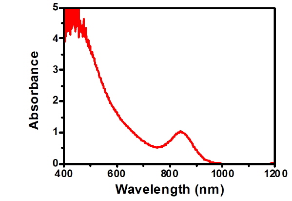
We prepared PbS CQD as described previously [14], a typical absorption spectrum of which is shown in Fig. 1.
2.1. Device Fabrication for SCLC Characterization
Within a N2-filled glove box PbS QD solar cells were fabricated using a layer-by-layer spin-coating technique onto ITO substrates, which were pre-cleaned by sonication for 10 minutes sequentially in acetone, methanol, and de-ionized (DI) water. PbS QDS (10 mg ml−1 in octane) was coated on the substrate by a spin coating method with 2500 rpm, which was treated by MPA (1 vol. % in methanol) and subsequently rinsed by methanol. This coating cycle was repeated around 10 times until the thickness of the overall PbS QDS layer became 100 nm, which was estimated by cross-sectional FE-SEM. The films were further annealed at 90℃ for 5 min in air. Finally, a thin LiF layer of 1 nm and Al back electrode of 200 nm were sequentially deposited on the PbS QDS layer using a thermal evaporator.
2.2. Heterojunction PbS QD Solar Cells Fabrication
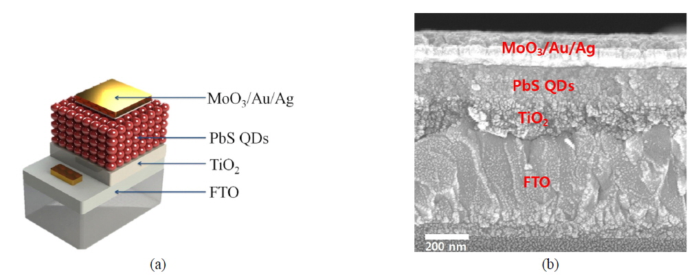
TiO2 layers were prepared by spin coating TiO2 paste (Solarronix, Ti-Nanoxide, HT/SC) on fluorine-doped tin oxide (FTO) substrate at 3,000 rpm and annealing at 450 ℃ for 30 min. PbS QDs layers were then fabricated using layer-by-layer spin-coating methods using PbS QDs (60 mg ml−1 in octane) and MPA (1 vol.% in methanol) as described previously [14]. The films were further annealed at 90 ℃ for 5 min in air. Finally, a MoO3 layer of about 10 nm and Au/Ag back electrode of 50/150 nm were sequentially deposited using a thermal evaporator. Six solar cells were fabricated in one batch experiment to consider characteristic variation.
Absorption spectra of PbS QDs in trichloroethylene (TCE) solutions and solar cells were measured by ultraviolet-visible (UV-VIS) spectroscopy (Shimadzu, UV3600) using an integrating sphere. Current-voltage (I-V) curves were measured using a Keithley 2400 source meter. A solar simulator (94023A, New port INC) with a 450W Xe lamp light source operating at 100 mW cm−2 as calibrated by a standard silicon solar cell was used to simulate the solar spectrum under AM1.5G conditions. External quantum efficiency (EQE) measurements were conducted on a custom built set-up (SPIQE200-5327, New port INC) which consists of 300W Xe lamp, a power supply, a monochrometer generating 20 nm band width, and a Merlin lock-in amplifier. A beam size of 0.01 cm2 was used to excite solar devices with active area of 0.09 cm2. All current-voltage and EQE measurements were carried out in an N2 environment.
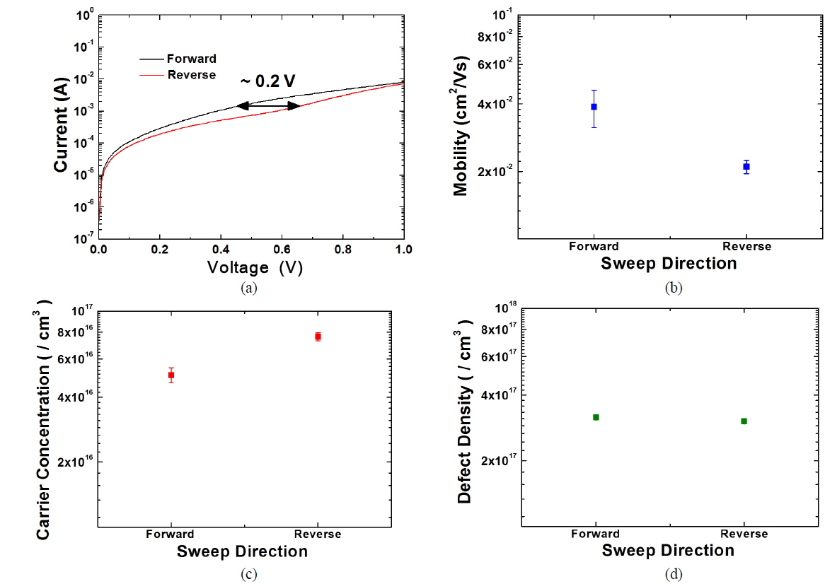
Space charge limited conduction (SCLC) governs charge transport in very thin QDS films, where QDS is thin enough to provide formation of percolation paths [13]. That is, the device for the characterization of SCLC needs to be nonrectifying, and therefore, the heterojunction solar cell structure cannot be used for the SCLC characterization. This behaviour gives a useful tool for characterizing charge carrier mobility, carrier concentration, and trap density related to the transport in a direct way from simple I-V measurements. We have fabricated ITO/PbS QDS/Al structure with 100 nm thick PbS QDS, and measured I-V characteristics to extract above-mentioned parameters according to the model described before [13]. The parameter extraction was based on the single trap SCLC model, where hole unipolar drift transport was assumed. We have found hysteretic I-V behaviour as shown in Fig. 2(a), which is physically related to the efficiency measurement problems recently issued for assessing emerging solar cells based on quantum dots [12] or perovskite materials [15]. The physical mechanism may be related to free carrier trapping or bound charge polarization, and in any case, it would be reasonable to assume a change in the electrostatic energy barrier to explain the hysteresis. The voltage shift in the hysteresis is found to be around 0.2 V, which corresponds to 0.7×1017 cm−3 volume charges if we assume uniform volume charges (in this calculation, the dielectric constant of the PbS QDS was 15 [13]). This may be related to the volume trap density, if most of the traps are filled with free carriers; however, this is smaller than the value obtained from SCLC analysis implying partially filled trap sites in hysteresis sweep. The mobility values show the order of 10−2 cm2/Vs as shown in Fig. 2(b), where they exhibit a slightly smaller value in the reverse sweep. Smaller extracted mobility in the reverse sweep may be due to the electrostatic scattering due to trapped charges. The carrier concentration shown in Fig. 2(c) exhibits an opposite trend, where a slightly larger extracted carrier concentration from the reverse sweep may be due to additional participation of detrapped charges in the current flow. The extracted trap density from SCLC analysis in Fig. 2(d) is around 3×1017 cm−3, which may be a more\exhibits an opposite trend, where a slightly larger extracted carrier concentration from the reverse sweep may be due to additional participation of detrapped charges in the current flow. The extracted trap density from SCLC analysis in Fig. 2(d) is around 3×1017 cm−3, which may be a more reasonable value than that from the I-V hysteresis shown above.
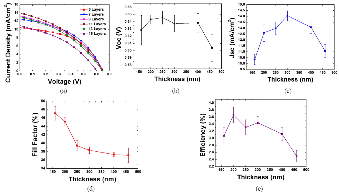
Solar cells with various PbS QDS thicknesses were fabricated as shown in Fig. 3 (a) and (b), which give a series of photovoltaic performances as shown in Fig. 4. The increase of\the thickness monotonically reduces fill factor (FF), while open circuit voltage (Voc) and short circuit current density (Jsc) increase up to a critical thickness and decrease again with a thickness thicker than the critical thickness. Similar thickness dependent behaviours have been reported before in PbS based quantum dot solar cells [1, 13] before, and the critical thickness that determines the Jsc is thought to be the onset thickness of full depletion. From Fig. 4(b) and (c), the onset thickness of full depletion is around 300 nm, above which, the dominant carrier collection mechanism switches from drift to diffusion.
The critical thickness that represents the thickness dependence of conversion efficiency has a functional relationship with the carrier diffusion length [1]. The critical thickness around 250 nm in this experiment roughly corresponds to the characteristics with diffusion length around 50 nm in Sargent’s work [1]. Once diffusion length (ldiff) is known, and we know that the internal electric field (Eint) that brings carrier drift is about 2~3×10⁴ V/cm, we can also estimate drift length (ldrift) to be around 200 nm (ldrift = ldiff2 Eint/(kT/q), where k, T, and q are Boltzmann constant, temperature and unit charge.). The estimated drift length is smaller than the onset thickness of full depletion, which shows that the thickness 250 nm of maximum efficiency (from the fitted graph) is even thinner than the onset thickness of full depletion. This is also related to the drastic reduction of FF with the thickness increase from 200 nm to 250 nm, while the FF variation in Sargent’s work is more gradual [1]. In their work, diffusion length was estimated to be 100 nm, which corresponds to the drift length of 800 nm. The drift length of amorphous Si solar cells is about ten times the cell thickness [16], which implies that the QDS with atomic passivation still needs three to four times improvement in its drift length to be compatible with state-of-the-art
Material quality of current QDS thin film is still below commercial photovoltaic materials as discussed above. The representative measure of the quality, drift length (or diffusion length) needs to be improved three to four times over that with current technology. Noting that the drift length is proportional to the product of mobility μ and carrier lifetime τ, and if we want to improve the drift length without a further improvement in QD surface passivation; we can obtain the improvement by controlling QD-to-QD distances [17] and their distributions [18]. For example, the average QD-to-QD distance and their stacking orderness can be reduced by low temperature annealing [19]. More sophisticated processing in coating or post-coating treatment would lead to a higher mobility through more compact stacking of QDs. Maybe in addition, the device structure ought to follow
We have investigated charge transport characteristics of one-step MPA-treated-QDS thin films using the SCLC analysis and the thickness dependent photovoltaic performance assessment. The current level of carrier drift mobility was estimated to be low-10−2 cm2/Vs with the diffusion length about 50 nm. The state-of-the-art QDS quality with two-step passivation is known to exhibit two times larger diffusion length, which is still to be improved three to four times in comparison with commercial photovoltaic materials like amorphous Si. A further development in coating method to optimize QD stacking would enable photovoltaic quality QDS compatible with other commercial photovoltaic materials.