검색 전체 메뉴
PDF
맨 위로
OA 학술지
A Polarization Diversity Patch Antenna with a Reconfigurable Feeding Network
  • 비영리 CC BY-NC
  • 비영리 CC BY-NC
ABSTRACT
A Polarization Diversity Patch Antenna with a Reconfigurable Feeding Network
KEYWORD
Polarization Diversity , Polarization Reconfigurable Antenna
  • I. INTRODUCTION

    Polarization diversity antennas are now well recognized for their low fading loss (which is detrimental to performance), as well as their high spectral efficiency [1]. Therefore, they have been used for wireless communication and sensor systems. Generally, a sensor system may have a pair of linearly polarized antennas and the polarization is selected by a switching circuit controlled by the baseband of the communicator to achieve the best signal quality [2]. However, this approach requires a large amount of space. A reconfigurable antenna with polarization diversity has an advantage of creating two or more polarizations using only one resonator [3-6]. In [3], four diodes were used for polarization diversity.

    However, this complicates the antenna structure. In [4], a polarization reconfigurable slot antenna was proposed where the vertical and horizontal linear polarizations were controlled by two PIN diodes. Nevertheless, an inherent bidirectional radiation generally occurs in slot antennas, which is undesirable in wireless communication applications [5]. In [6], a reconfigurable patch antenna was proposed that had a U-shaped feeding structure for switching the polarization between the right-hand circular-polarization (RHCP) and the left-hand circular-polarization (LHCP). However, this antenna requires a multi-layer structure.

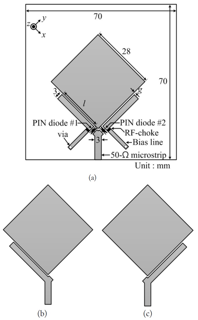
    A previous publication introduced a square-patch antenna with an asymmetric Y-shaped feed structure for circular polarization [7]. This idea, with two PIN diodes inserted in the gap between the patch and the Y-shaped feed line, was proposed in [8] for polarization diversity. As a result, polarization can be switched between LHCP and RHCP. The present letter proposes a structure that differs from that in [7]; namely, a novel reconfigurable patch antenna for linearpolarization (LP) diversity. Ideally, the Y-shaped feed structure can be changed into one of the shapes in Fig. 1(b) and (c) when only one of the two PIN diodes is in the on-state. This brings about the LP radiation of the square-patch antenna.

    II. ANTENNA DESIGN

    The configurations of the proposed reconfigurable antenna and the ideal cases according to the bias states of the two PIN diodes are illustrated in Fig. 1. The proposed reconfigurable patch antenna is fabricated on a commercially available FR-4 dielectric substrate with a permittivity of 4.2 and a thickness of 1.6 mm. The size of the ground plane is 70 × 70 mm2 and it is printed on the bottom layer. The proposed antenna mainly consists of a square patch and a Yshaped feed structure with two PIN diodes. The side length of the square patch is 28 mm. The lengths of the two branch lines of the Y-shaped feed structure are equal and are denoted by l, with a width of 1.5 mm each. The gap between the square patch and the branch lines is denoted by g. The two PIN diodes (#1 and #2, part number: HSMP-3860) are inserted into the feed structure. The PIN diodes operate at 0.75 V, and they consume a current of 3 mA. When PIN diode #1 is in the on-state and #2 is in the off-state, a positive voltage is supplied to PIN diode #1 through the 50-Ω microstrip line, while a negative voltage is supplied through the system’s ground plane. When PIN diode #1 is in the off-state and #2 is in the on-state, the positive and negative voltages are reversed.

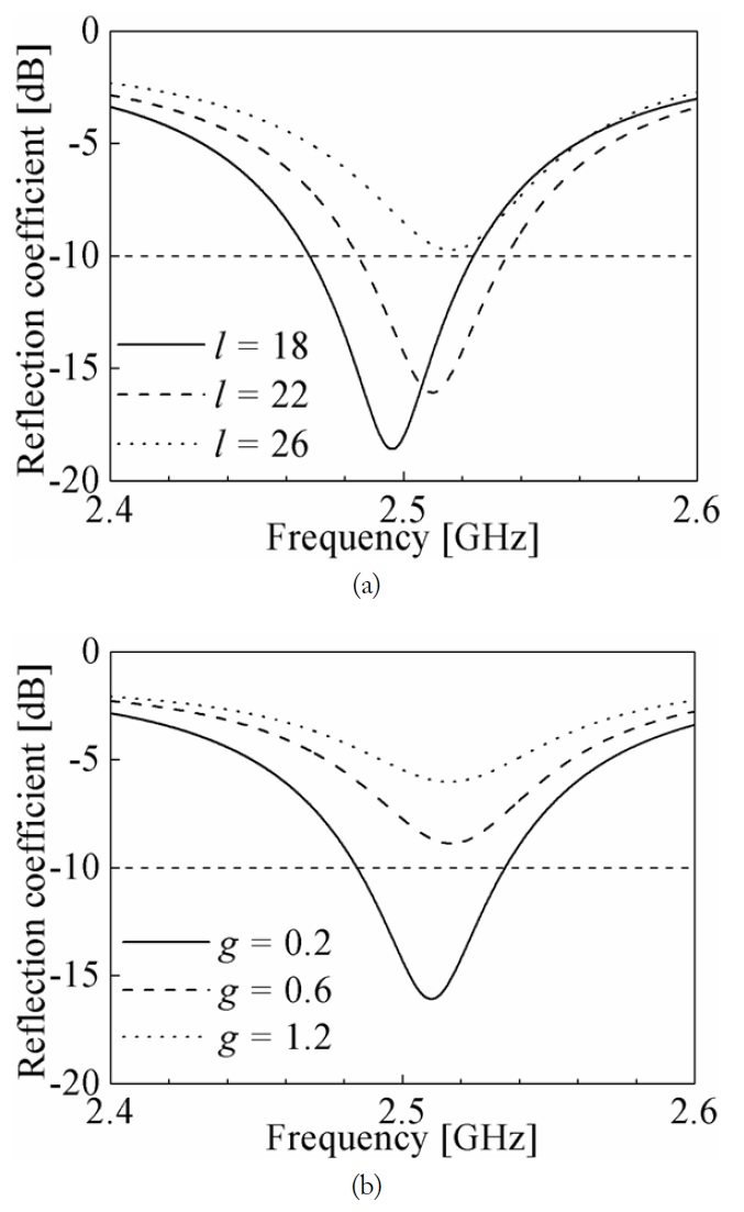
    Fig. 2 shows the simulated results of the proposed antenna in accordance with the variations in l and g, when PIN diode #1 is in the on-state and #2 is in the off-state. The other parameters for the simulation are equivalent to those provided in Fig. 1. As shown in Fig. 2(a), the resonant frequency of the proposed antenna is shifted to lower frequency by decreasing l. This is owing to the coupling between the patch and the branch line. On the other hand, the impedance matching of the resonant frequency deteriorates with increasing g. This is because the degree of coupling between the square patch and the branch lines is weakened by increasing g. In this study, l and g are set to 22 mm and 0.2 mm, respectively, to create the widest 10-dB impedance bandwidth.

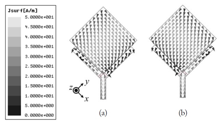
    Fig. 3 shows the simulated current distribution on the square patch surface at 2.51 GHz. When PIN diode #1 is in the on-state and #2 is in the off-state, maximum current density is observed along the y-axis. In this case, little current density occurs at the right branch of the Y-shaped structure because diode #2, in the off-state, properly blocks the radiofrequency (RF) power. On the other hand, maximum current density is observed along the x-axis when PIN diode #1 is in the off-state and #2 is in the on-state. This confirms that the polarization sense of the proposed antenna is controlled by adjusting the bias states of the two PIN diodes. Note also, as shown in Fig. 3, that the minimum current density exists at the bias circuit. This means that the RF signal is properly isolated from the DC bias.

    III. SIMULATED AND MEASURED RESULTS

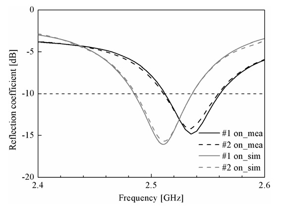
    Fig. 4 shows the simulated and measured reflection coefficients of the proposed antenna. The geometric dimensions of the proposed antenna are l = 22 mm and g = 0.2 mm. Other dimensions are the same as those shown in Fig. 1. The proposed antenna has a 10-dB impedance bandwidth of 1.97 %. The measured results are slightly increased due to the dielectric constant mismatch.

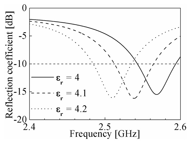
    Fig. 5 shows the simulated reflection coefficient of the proposed antenna according to variation of εr when PIN diode #1 is in the on-state and #2 is in the off-state. The resonance of the proposed antenna is shifted to a lower frequency by increasing εr. The resonance at εr = 4.1 almost matches the measuring resonance. This simulation result shows that a frequency deviation of about 20 MHz occurs between the simulation and measurement due to the dielectric mismatch.

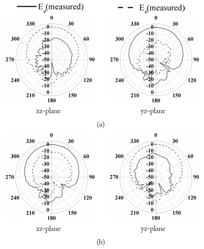
    Fig. 6 shows the measured 2D radiation patterns of the proposed antenna. The measured peak gain is 3.13 dBi when PIN diode #1 is in the on-state and #2 is in the off-state. On the other hand, the measured peak gain is 3.03 dBi when PIN diode #1 is in the off-state and #2 is in the on-state. In both the cases, the cross-polarization levels are better than -16 dB and -13.2 dB, respectively. The measured results show that broadside radiation patterns with good LP characteristics are obtained. In the xz-plane of Fig. 6(a), the copolarization is |Eθ|, while the co-polarization is |Eφ | in the xz-plane of Fig. 6(b). These results confirm that a polarization-switching technique has been developed for microtrip patch antennas.

    IV. CONCLUSION

    This paper proposes a reconfigurable patch antenna for LP diversity. Two LPs, which are orthogonal to each other, can be switched by using two PIN diodes. A prototype of the proposed design is successfully implemented and the simulated and measured results concurred. The proposed antenna is suitable for applications in communication and sensor systems.

참고문헌
  • 1. Kim B., Pan B., Nikolaou S., Kim Y. S., Papapolymerou J., Tentzeris M. M. 2008 "A novel single-feed circular microstrip antenna with reconfigurable polarization capability," [IEEE Transactions on Antennas and Propagation] Vol.56 P.630-638 google cross ref
  • 2. Sung Y. J. 2012 "Frequency and polarisation reconfigurability from an open-loop square ring antenna," [IET Microwaves, Antennas & Propagation] Vol.6 P.505-509 google cross ref
  • 3. Liu W. L., Chen T. R., Chen S. H., Row J. S. 2007 "Reconfigurable microstrip antenna with pattern and polarisation diversities," [Electronics Letters] Vol.43 P.77-78 google cross ref
  • 4. Li Y., Zhang Z., Chen W., Feng Z. 2010 "Polarization reconfigurable slot antenna with a novel compact CPWto-slotline transition for WLAN application," [IEEE Antennas and Wireless Propagation Letters] Vol.9 P.252-255 google cross ref
  • 5. Rao Q., Denidni T. A., Johnston R. H. 2004 "A singlesubstrate microstrip-fed slot antenna array with reduced back radiation," [IEEE Antennas and Wireless Propagation Letters] Vol.3 P.265-268 google cross ref
  • 6. Tong K. F., Huang J. 2008 "New proximity coupled feeding method for reconfigurable circularly polarized microstrip ring antennas," [IEEE Transactions on Antennas and Propagation] Vol.56 P.1860-1866 google cross ref
  • 7. Sung Y. J. 2010 "Circularly polarised square patch antenna with asymmetrical Y-shaped feed structure," [Electronics Letters] Vol.46 P.1309-1310 google cross ref
  • 8. Sung Y. J. 2013 "Polarisation diversity antenna with asymmetrical Y-shaped feed structure," [Electronics Letters] Vol.49 P.1512-1513 google cross ref
OAK XML 통계
이미지 / 테이블
  • [ Fig. 1. ]  Configurations of the proposed structure: (a) proposed antenna, (b) ideal case when only PIN diode #1 is in the on-state, and (c) ideal case when only PIN diode #2 is in the on-state.
    Configurations of the proposed structure: (a) proposed antenna, (b) ideal case when only PIN diode #1 is in the on-state, and (c) ideal case when only PIN diode #2 is in the on-state.
  • [ Fig. 2. ]  Simulated reflection coefficient of the proposed antenna when the PIN diode #1 is in the on-state and #2 is in the off-state (a) variation according to l and (b) variation according to g.
    Simulated reflection coefficient of the proposed antenna when the PIN diode #1 is in the on-state and #2 is in the off-state (a) variation according to l and (b) variation according to g.
  • [ Fig. 3. ]  Simulated current distribution (a) PIN diode #1 is in the onstate and #2 is in the off-state, (b) PIN diode #1 is in the offstate and #2 is in the on-state.
    Simulated current distribution (a) PIN diode #1 is in the onstate and #2 is in the off-state, (b) PIN diode #1 is in the offstate and #2 is in the on-state.
  • [ Fig. 4. ]  Simulated and measured reflection coefficient of proposed antenna.
    Simulated and measured reflection coefficient of proposed antenna.
  • [ Fig. 5. ]  Simulated reflection coefficient of the proposed antenna according to variation of εr when PIN diode #1 is in the on-state and #2 is in the off-state.
    Simulated reflection coefficient of the proposed antenna according to variation of εr when PIN diode #1 is in the on-state and #2 is in the off-state.
  • [ Fig. 6. ]  Measured 2D radiation pattern (a) PIN diode #1 is in the onstate and #2 is in the off-state, and (b) PIN diode #1 is in the off-state and #2 is in the on-state.
    Measured 2D radiation pattern (a) PIN diode #1 is in the onstate and #2 is in the off-state, and (b) PIN diode #1 is in the off-state and #2 is in the on-state.
(우)06579 서울시 서초구 반포대로 201(반포동)
Tel. 02-537-6389 | Fax. 02-590-0571 | 문의 : oak2014@korea.kr
Copyright(c) National Library of Korea. All rights reserved.