Electromagnetic wave propagation in any medium obeys the fundamental physical laws described by Maxwell’s equation [1]. Most media exhibit normal propagation called subluminal, where the speed of propagation of individual timeharmonic components is slower than the speed of light, c, in a vacuum at all frequencies. However, in a specific and narrow frequency band of signal attenuation (SA) or in an anomalous dispersion frequency, the group velocity is observed to be greater than the c. This abnormal wave propagation is called superluminal group velocity or even negative group velocity [1,2].
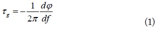
The wave propagation in any medium can be characterized by group velocity and group delay (GD), which are same. The GD in a circuit can be investigated by examining transmission phase variation with respect to frequency and can be defined as a negative derivative of the signal transmission phase according to frequency, as shown in (1).
As seen from (1), when quantity τg is positive, the peak of the output pulse suffers a positive delay with respect to input pulse. On the other hand, if τg is negative, the peak of the output pulse emerges prior to the peak of the input pulse entering the medium, and the medium is said to exhibit a negative GD [3]. However, this does not violate the causality because the initial transient pulse is still limited to the front velocity, which will never exceed the speed of light [4].
The negative group delay (NGD) occurs at a certain range of frequency where the absorption or SA is maximum [1]. Therefore, band-stop structures are used to realize NGD circuits. Based on either series or shunt RLC resonators, various kinds of microwave NGD circuits have been presented and demonstrated in the literature [5-13]. To overcome the limited feasibility problem of lumped elements in microwave frequencies, the NGD circuits using distributed elements are also presented [5-7,12]. However, the conventional NGD circuits presented in previous works exhibited excess SA up to 35 dB for a -8 ns GD, which can cause serious stability issues when an NGD circuit is integrated with RF/microwave systems. Therefore, for the same GD, the passband SA must be as small as possible.
A few studies have been conducted about NGD networks with small SA. In [13], a composite NGD network with smaller SA was presented. However, this circuit requires parallel lumped elements (such as capacitors and inductors) between two transmission lines, making implementation difficult at microwave frequencies.
In this paper, a design of the transmission line NGD circuit with reduced SA and multiple pole GD characteristics is presented.
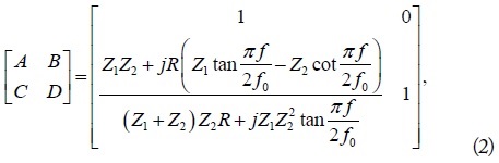
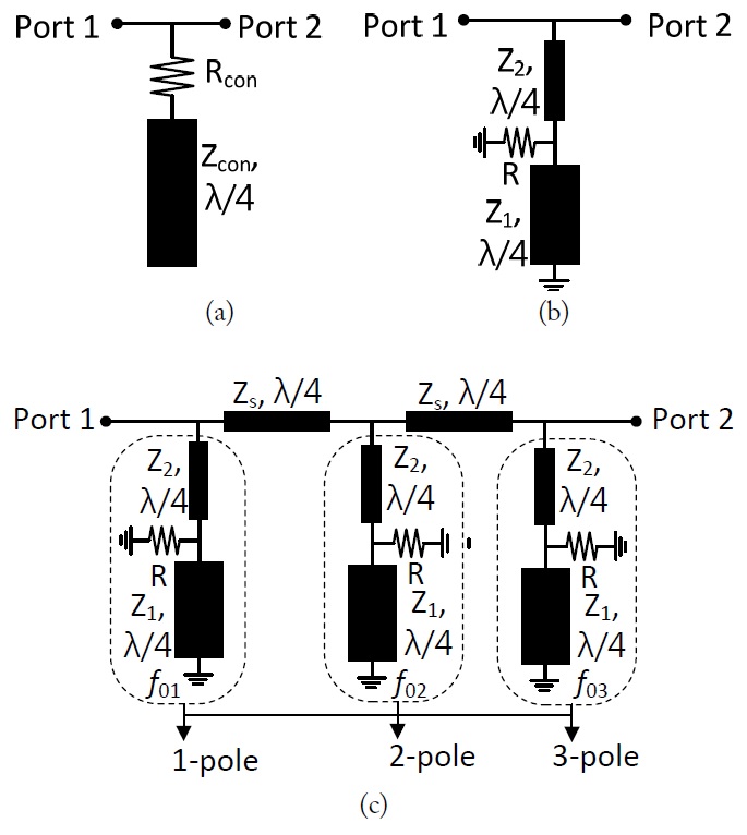
Fig. 1 shows the structure of the conventional and proposed 1-pole NGD circuits that consist of resistor R and transmission lines with characteristic impedances of Z1 and Z2 and electrical lengths of λ/4. Total ABCD-parameters of the proposed circuit shown in Fig. 1(b) can be found as (2)
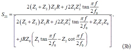
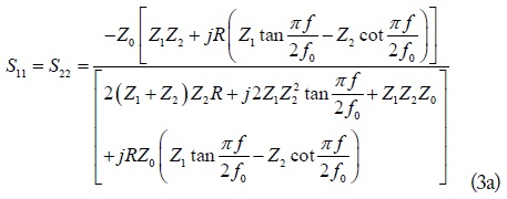
where f and f0 are operating and design center frequencies, respectively. The S-parameters of the proposed circuit can be found by using ABCD- to S-parameters conversion relationship [14], which is given as (3):
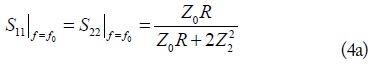
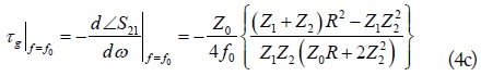
where Z0 is reference port impedance. Furthermore, S-parameters and GD at the f0 can be obtained as (4).
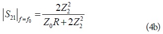
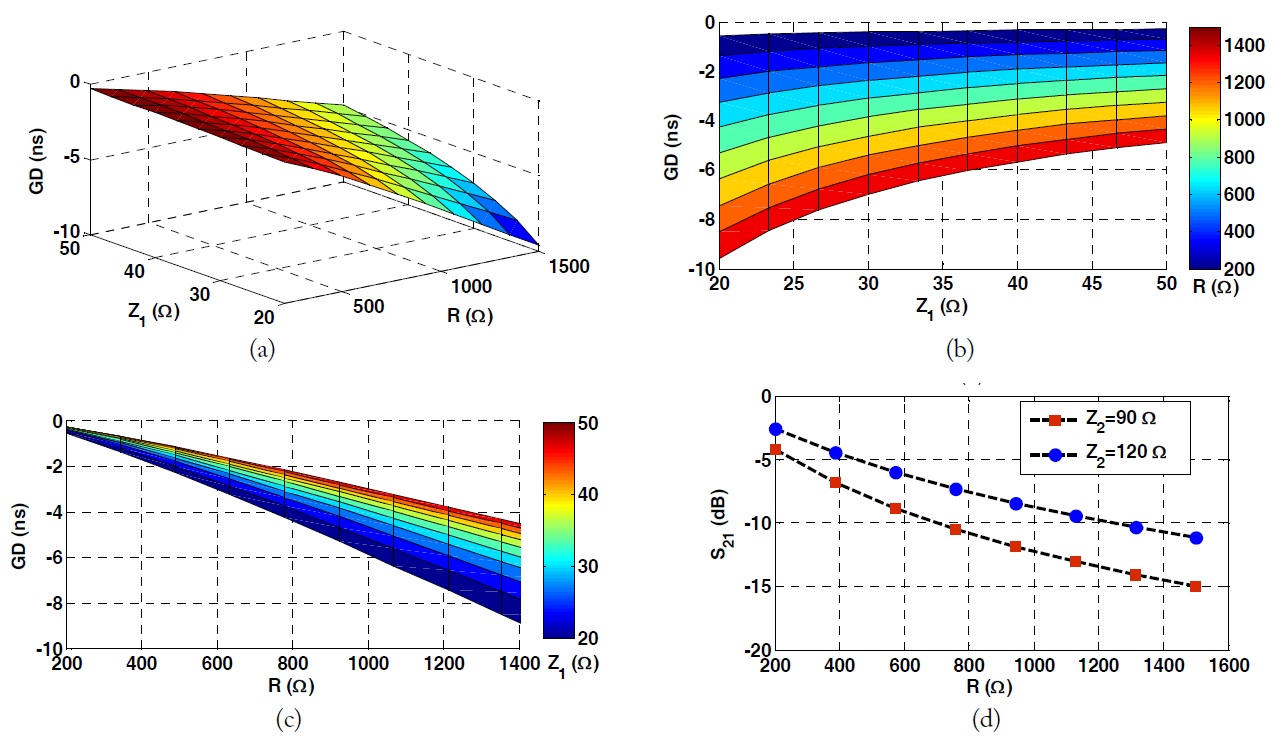
As seen from (4c), the maximum achievable GD depends on Z1, Z2, and R. To better understand (4b) and (4c), the calculated maximum achievable GD and SA at f0 = 1.96 GHz according to Z1 and R are shown in Fig. 2. As seen from this figure, the SA is improved as Z2 increases. Therefore, high Z2 and low Z1 are necessary for reduced SA.
Fig. 3 shows the simulation results of the 1-pole NGD circuit. In this simulation, the maximum achievable GD at f0 = 1.96 GHz is assumed to be -5 ns. As seen from this figure, the proposed circuit provides reduced SA as compared to the conventional circuit [6]. The SA of the proposed circuit is further reduced by making the value Z2 is high. However, the NGD bandwidth is reduced.
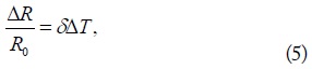
The temperature dependence of R is represented by the following relationship:
where δ, R0, ΔR, and ΔT are temperature coefficient, initial resistance, resistance variation, and temperature variation, respectively.
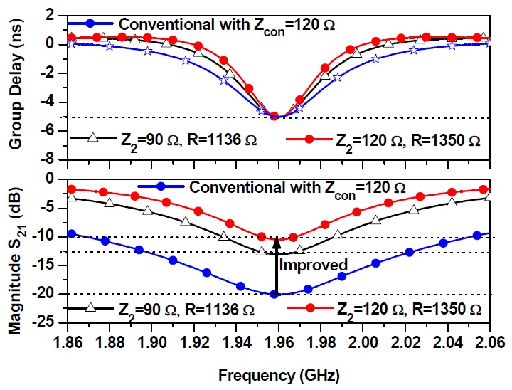
Fig. 4 shows the performance degradation of the proposed 1-pole NGD circuit, assuming the resistance variation of ±5%. As seen from this figure, the GD and SA (magnitude of S21) variations are approximately ±0.61 ns and ±0.68 dB from the reference values. These results indicate that the proposed NGD circuit is considerably less sensitive to the temperature-dependent resistance variation.
The NGD bandwidth can be enhanced by connecting 1-pole NGD circuits with the slightly different center frequencies (f0i, i = 1, 2, 3, …) separated by λ/4 transmission lines with characteristic impedance of Zs = 50 Ω, as shown in Fig. 1(c). Due to the different f0 of 1-pole NGD circuits, multiple pole GD characteristics can be obtained.
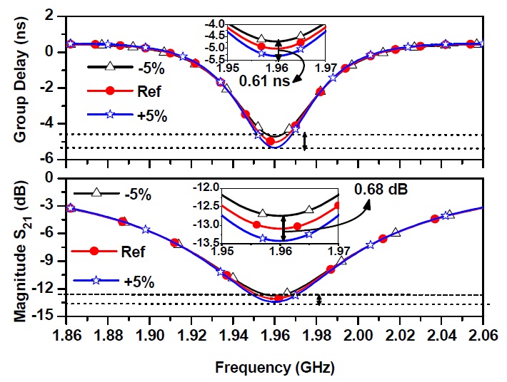
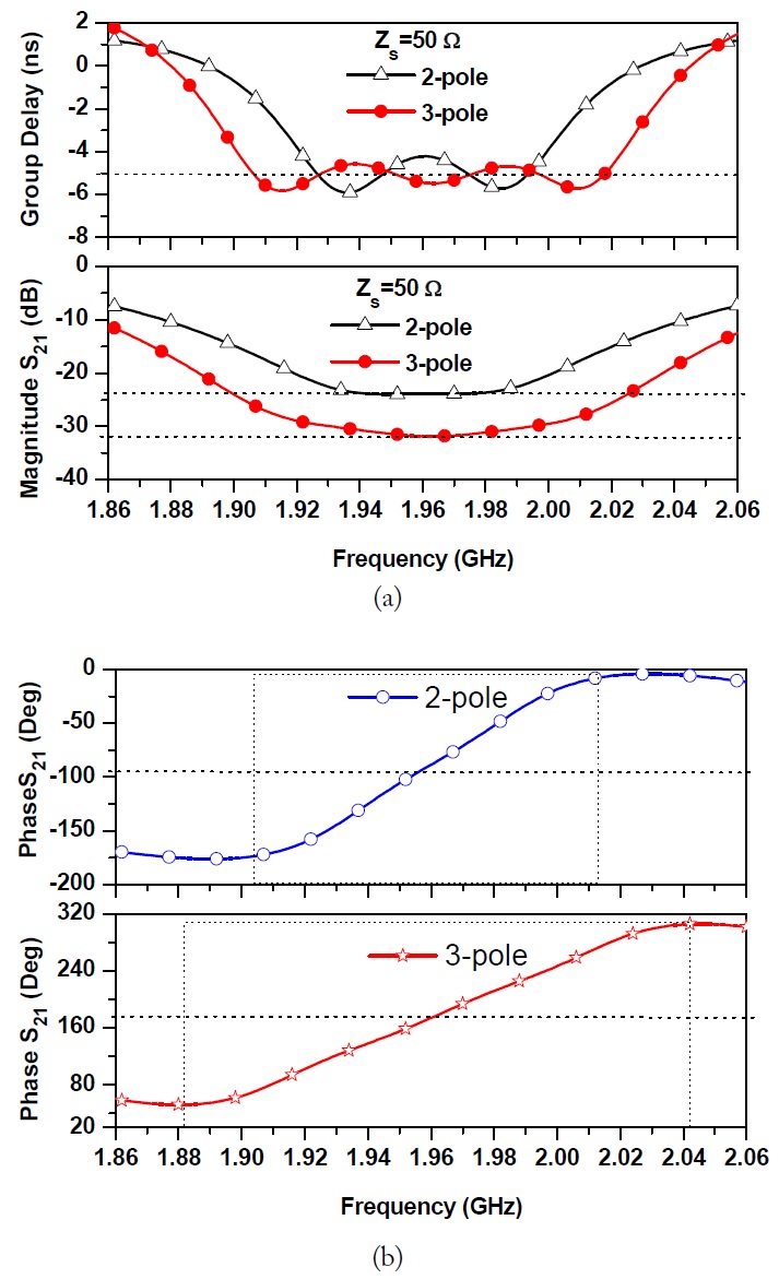
Fig. 5(a) shows the simulated GD and S21 magnitude results of 2-pole and 3-pole NGD circuits. In the case of a 2-pole NGD circuit, two NGD circuits with f01 = 1.935 GHz and f02 = 1.984 GHz are cascaded. Similarly, for the 3-pole NGD circuit, the f0i are given as f01 = 1.912 GHz, f02 = 1.963 GHz, and f03 = 2.03 GHz. In both cases, the circuit element values of 1-pole NGD circuits are given as Z1 = 30 Ω, Z2 = 90 Ω, and R = 1139 Ω. As seen from these figures, the NGD bandwidth is enhanced due to 2-pole and 3-pole characteristics. The phase characteristics of 2-pole and 3-pole NGD circuits are shown in Fig. 5(b). As seen from this figure, the phase slope of S21 is positive over a certain range of frequency, which signifies the presence of NGD characteristics.
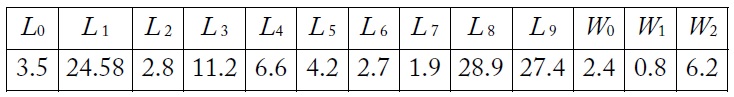
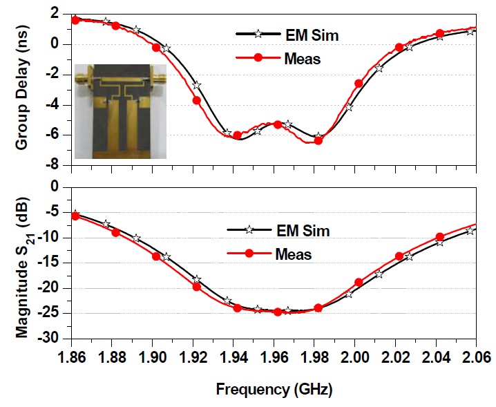
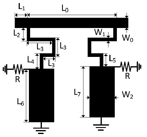
For experimental validation of the proposed circuit, the design goal was to obtain a GD of -6 ns at f0 = 1.96 GHz. For this purpose, a 2-pole NGD circuit was designed and fabricated. For given specifications, the calculated circuit element values of a 2-pole NGD circuit are given as Z1 = 30 Ω, Z2 = 90 Ω, Zs = 50 Ω, and R = 1,140 Ω. The f0s are the same as presented in Section II. The circuit was fabricated using RT/Duroid 5880 of Rogers Inc. with a dielectric constant (εr) of 2.2 and the thickness (h) of 31 mils. The simulation was performed using ANSYS HFSS 2014. The layout of the fabricated circuit is shown in Fig. 6. The physical dimensions of the fabricated circuit are shown in Table 1 after the optimization.
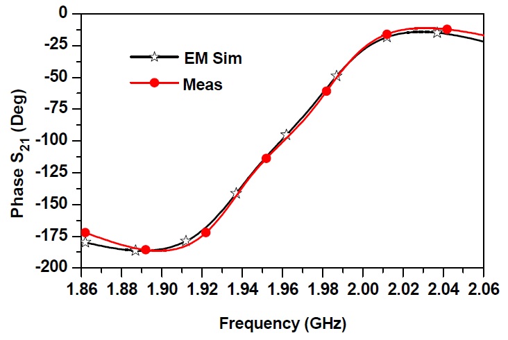
Fig. 7 shows the simulated and measured GD and magnitude results of the 2-pole NGD circuit. From the measurement, the GD was determined as -5.80±0.45 ns over a bandwidth of 80 MHz. The maximum SA at f0 = 1.962 GHz was 24.67 dB. The SA can be easily compensated using general purpose gain amplifiers [5]. A photograph of the fabricated circuit is also shown in Fig. 7. The simulated and measured phase characteristics are shown in Fig. 8. As seen in this figure, the slope of the phase is positive over a certain region. This positive phase slope characteristic can be used to cancel out the negative phase slope to obtain zero GD or a phase-compensated response.
This paper demonstrates the design of an NGD circuit with multiple pole GD characteristics and reduced signal attenuation. The multiple pole NGD circuit is obtained by the cascade connection of several 1-pole circuits having slightly different frequencies. For the experimental verification, the 2-pole NGD circuit was designed, fabricated, and measured. The proposed topology can reduce the number of gain-compensating amplifier stages and can help improve efficiency, out-of-band noise reduction, and stable operations when integrated into RF/microwave systems.