The objective of this research is the realization of a highefficiency microwave heating system that uses a solid-state amplifier. The magnetron, which is a vacuum tube, is commonly used as a signal source in conventional microwave chemical reaction systems. The magnetron shows high efficiency at high output power, but its oscillating frequency and the output power are unstable, which leads to poor reliability for chemical reactions. The output power from a magnetron is conducted to the chemical chamber through a waveguide, but this does not necessarily lead to full power utilization. The actual absorption efficiency greatly depends on the material properties of the object being heated. A low absorption efficiency results in most of the power (e.g., more than half) being reflected to the magnetron and dissipated as heat.
This study presents a new technique to improve absorption efficiency by frequency and phase control. In addition, power from multiple antennas is combined by controlling the phase in the heating furnace. This is the largest advantage of a solid-state heating system, because a magnetron cannot control either the oscillation frequency or the phase of the output signal. The proposed system can control the frequency and phase with high accuracy through the use of a semiconductor device.
The high power amplifier (HPA) that uses the emerging technology of a GaN-HEMT (Gallium Nitride High Electron Mobility Transistor) can provide a high output power comparable to that of a magnetron. Current HPAs include the L-band 500 W [1] and S-band 800 W [2], but HPAs with output powers of more than 100 W have been reported even in the high frequency bands (C-, X- and Ku-bands) [3,4]. A power added efficiency (PAE) of 80% is achieved for output power of 16.5 W [5]. However, the efficiency of GaN-HEMT is somewhat lower than that of a magnetron for the condition of high output power with CW operation.
In recent years, harmonic processing techniques have been extensively studied in order to design high efficiency power amplifiers. Ideally, an efficiency of 100% can be obtained by a harmonic processing technique, such as class-F and inverse class-F, where the load impedances for harmonics are controlled as zero or infinity. However, the effects of parasitic elements in GaN-HEMT cause the optimum load impedances to deviate from the ideal impedances [6], thereby deteriorating the efficiency. This could be restored by optimizing the reflection phase of the harmonics, and past research has reported the use of field effect transistors (FETs) with internal or on-chip matching circuits [7,8]. However, a high efficiency power amplifier using a packaged external matching transistor has not yet been reported.
The present study describes the design of a 100-W GaNHEMT HPA that uses a large-signal model of a transistor and considers the reflection phases of the harmonics. The intention of the design is to incorporate the HPA into a microwave heating system.
The solid-state microwave heating system is constructed by designing and fabricating a 200-W power amplifier module. The developed heating system has a total of 400 W output power fed from two metal patch antennas installed on the top and bottom of the chamber. The frequency and phase in this system can be controlled electronically to realize highefficiency heating. Reflected power in the chamber is detected by a monitoring sensor in real time. This paper demonstrates the advantages of the solid-state microwave heating system, where the heating efficiency depends on frequency and phase.
II. LARGE SIGNAL SIMULATION OF GAN-HEMT
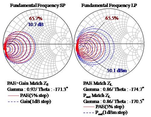
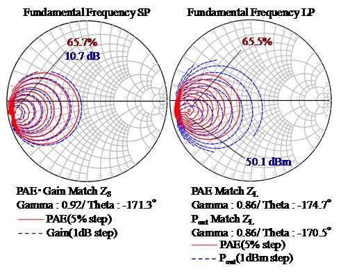
The GaN-HEMT used in this study is a CGH40120F, which is a GaN on SiC device manufactured by Cree. Fig. 1 shows the characteristics of the source pull (SP) and load pull (LP) for a fundamental frequency wave, using a large-signal model provided by Cree. Advanced Design System (by Keysight) is used in circuit simulation. The non-linear simulation yields an output power (
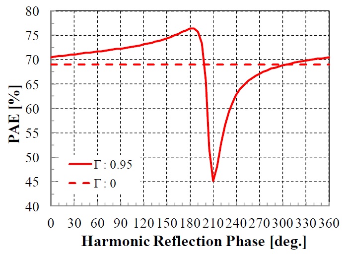
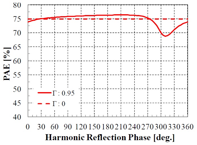
Fig. 2 shows a setup for simulation and measurement of harmonic load-pull and source-pull. This is often performed using a mechanical tuner (for example, the Focus microwave PHT tuner etc.), but this research calculates the dependencies of PAE on the reflection phases of the second and third harmonics by a load-pull simulation. Figs. 3 and 4 show that PAE is improved by 10% near the reflection phase of 170° for the 2nd harmonic, while the improvement for the 3rd harmonic is small. Thus, the reflection phase of 3rd harmonic is set to the angle, at which the efficiency is not deeply degraded. The optimum impedances, including the fundamental wave, are listed in Table 1.
[Table 1.] Simulated optimum impedances
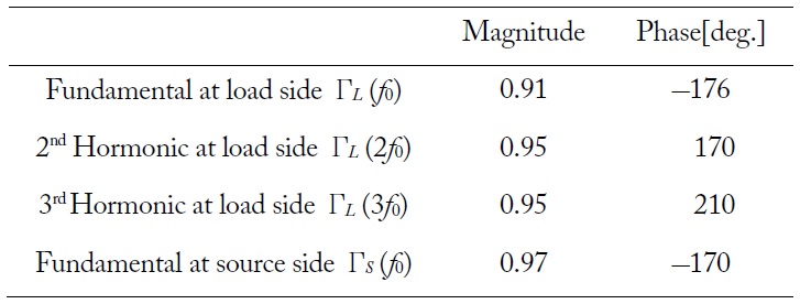
Simulated optimum impedances
III. DESIGN OF POWER AMPLIFIER
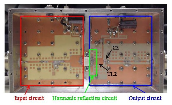
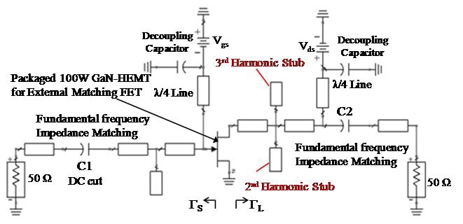
A schematic of the amplifier circuit is shown in Fig. 5. The harmonic reflection circuit is connected to the drain of the transistor. The harmonics at the gate side have little effect on efficiency. Thus, input matching is considered only for the fundamental frequency. The designed circuit and pattern for harmonic reflection are shown in Fig. 6.
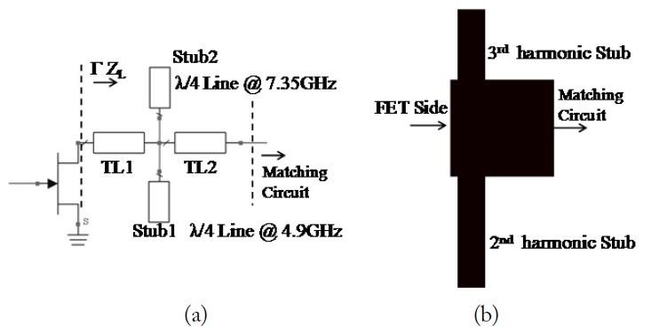
In Fig. 6(a), the open stubs (Stub1, Stub2) of the quarter-wavelength for each harmonic are used for harmonic processing. The reflection phase is controlled by the length of the transmission line TL1. The widths of TL1 and TL2 are set to 7 mm based on the electrode terminal size of the FET; this corresponds to a characteristic impedance of 17.7 Ω. The reflection phase of the second harmonic is mainly determined by TL1 and is set to the optimal value of 2.59°, in terms of the fundamental wave. Fortunately, this length was not a length where the reflection phase of third harmonic degrades the efficiency. If changes are desired in the reflection phase of third harmonic, the connection points for the second and third harmonics should be separated. The impedance for the fundamental wave is controlled by the length of TL2 and the capacitor (C2). The length of TL2 is set to 54.6°, and C2 is set to 1.1 pF.
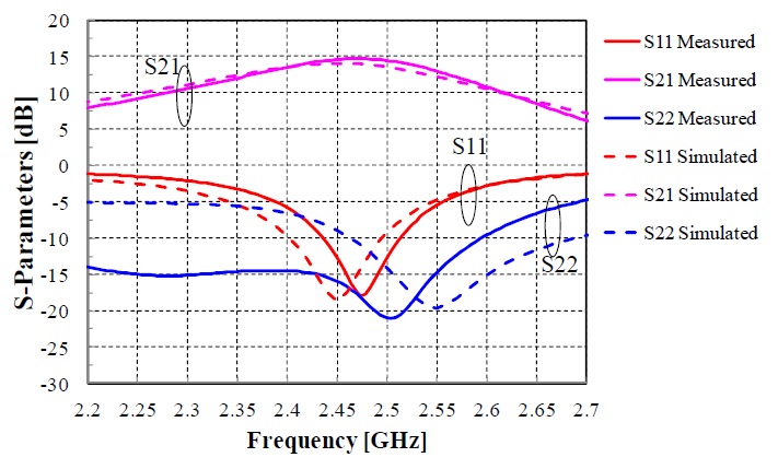
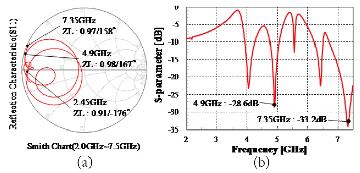
Fig. 6(b) shows a pattern designed by electromagnetic field analysis, corresponding to circuit analysis. Its reflection characteristics and transmission characteristics are shown in Fig. 7(a) and (b). The respective impedances (
IV. MEASURED CHARACTERISTICS OF THE AMPLIFIER
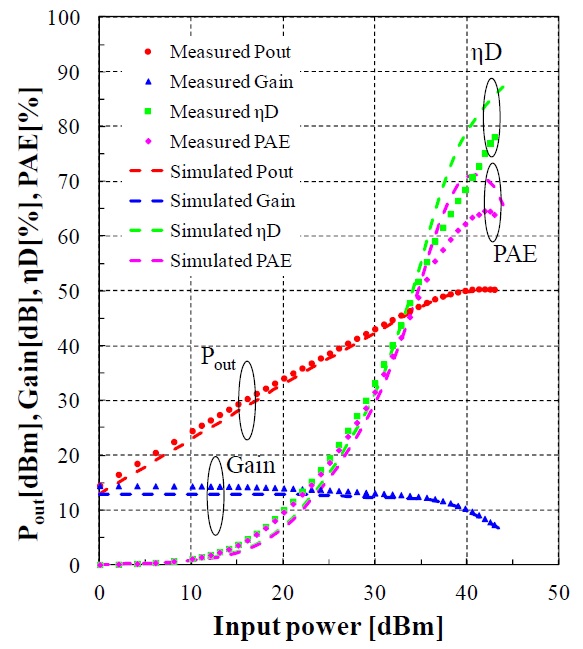
A photograph of a prototype 100 W GaN HPA is shown in Fig. 8. The simulation was carried out using the nonlinear large signal model provided by Cree. The simulated and measured input-output small-signal characteristics and large-signal characteristics are shown in Figs. 9 and 10. The bias conditions of the amplifier are
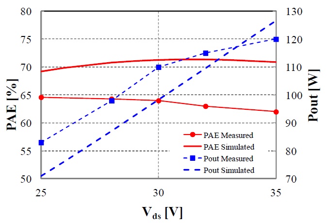
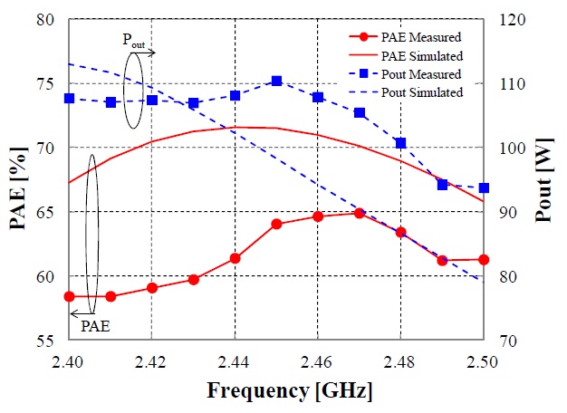
Fig. 11 shows the simulated and measured dependences of the output power and PAE on the drain voltage. The output power increases according to the drain voltage, but the efficiency is saturated and does not show further increases. An output power over 100 W is obtained at drain voltages higher than 28 V. An output power of 120 W was obtained, but the PAE was degraded to 62% so the reliability of the device might not be guaranteed. Fig. 12 shows the simulated and measured dependences of the output power and PAE on frequency. The measured output power is relatively higher and the efficiency is lower than for the simulation, so the impedance of the prototype circuit is more likely matched with the high power condition. Thus, PAE could be improved by modifying the load impedance, which deviated from the high efficiency condition.
V. SYSTEM DESIGN OF THE MICROWAVE HEATING SYSTEM
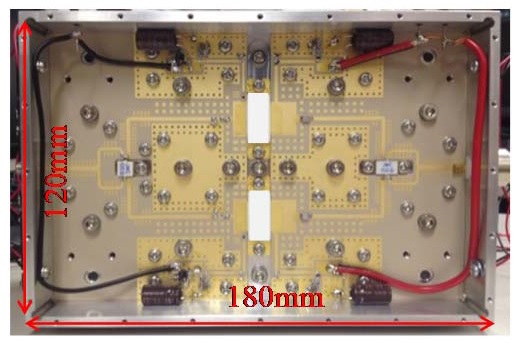
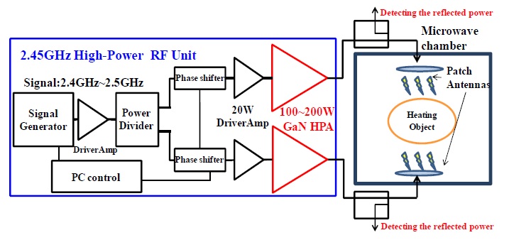
A microwave heating system was constructed using the developed amplifier. The heating system comprised two 200 W GaN HPA modules, in which the 100 W GaN HPAs are combined by Wilkinson combiners. Thus, the total maximum output power is 400 W, fed from two patch antennas mounted on the top and bottom of the heating chamber. Fig. 13 shows the prototype 200 W GaN HPA module. The size of the 200-W module is 180 mm by 120 mm; miniaturizetion has not yet been considered.
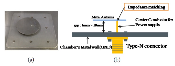
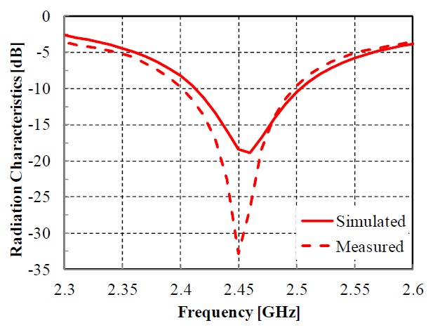
Fig. 14 shows the structure of the patch antenna for high power handling. The antenna has a metal-air structure, comprising a circular aluminum plate and a center conductor pin connected to the plate at its impedance matching point. This structure can handle up to a few hundred Watts. Fig. 15 shows the simulated and measured performances of the patch antenna in free space. The EMPro (by Keysight) is used for 3D electromagnetic field analysis; this antenna has relatively wide-band characteristics. The gain of the antenna is about 5 dB higher than that of a conventional patch antenna.
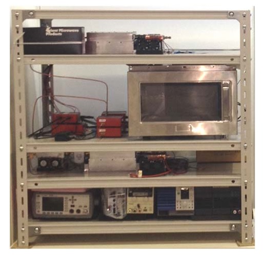
Fig. 16 shows a block diagram of the developed GaN mi-crowave heating system. The system consists of a signal generator, a power divider, variable phase shifters, variable attenuators, driver amplifiers, GaN HPAs, patch antennas, a heating chamber, reflected power sensors, and a control PC. The signal generator, variable phase shifters, and variable attenuators can be controlled electronically from the PC via USB connections. Fig. 17 shows a photograph of the constructed system.
At present, basic heating experiments have just been initiated and 100 mL of water in glass cup was successfully heated. The temperature of the water rose from 20℃ to over 90℃ in 90 seconds. An experiment to study chemical reactions was also carried out in which silver nano-particles were produced from an oxide solution by microwave heating.
Development of control software is underway. The experiments presented here were conducted manually, but a fully-automatic heating system will be constructed soon. The completed version of the system will allow automatic detection of the change in absorption efficiency.
The frequency and phase are then controlled by the control PC according to a predetermined algorithm. This type of operation is difficult for a magnetron. Thus, the authors believe that the GaN microwave heating system is very effective and represents a promising new technology.
A 2.45 GHz 100 W GaN-HEMT HPA with PAE of 64% was successfully designed and fabricated. Some difficulties encountered with high-power amplifiers, such as performance degradations due to parasitic elements, were overcome. The reflection phases of the harmonics were optimized by a precise design that used the large signal model of a GaN-HEMT. A prototype of a GaN microwave heating system was also developed. The total maximum output power was 400 W, which was fed from two patch antennas mounted on the top and bottom of the heating chamber. The frequency and phase can be controlled electronically to maximize absorption. The authors have initiated heating experiments and expect that this GaN microwave heating system could drastically improve the quality and productivity of chemical reactions. Therefore, this technology could reform the industry.
 80% PAE,"" href="http://dx.doi.org/10.1109/JSSC.2007.904317" target="_blank">