Oxide semiconductor which has been studied extensively as a semiconductor material has a wide band gap and high mobility. Amorphous oxide semiconductors (AOSs) such as ZnO-based thin film transistors (TFTs) have attracted much attention for their application to integrated circuits used in backplane of active matrix displays, because of their higher electrical and optical property than that of amorphous silicon thin film transistors (a-Si TFTs) and low production cost compared with the lowtemperature polycrystalline silicon (LTPS). The AOSs TFTs have shown high mobility due to their ns-orbital overlap structure. In addition, AOS thin-films have advantages of transparency in the visible range due to a large bandgap(~3.3 eV)[1-3]. Recently, there have been many reports on different active layer materials of AOSs TFTs. Among them, the material that is most extensively used currently is indium-gallium-zinc-oxide (IGZO) [4]. However, indium is an expensive and rare material, and indium-free materials, like zinc tin oxide (ZTO), have been studied intensively these days [5,6]. Because indium is not an abundant material, it is necessary to reduce indium usage for the future. Most of AOSs TFTs are annealed for the improvement of electrical performance and stability of device after deposition at room temperature (RT). Thermal annealing parameters are observed to be closely related with the annealing temperature and the ambient condition [7]. Therefore, it is very important to optimize the annealing process [8,9].
In this paper, we have fabricated zinc tin oxide (ZTO) TFTs without indium and compared them in the air and in wet and vacuum ambient with different annealing conditions. Followed by the completed fabrication of ZTO TFT, the performance of TFT has been compared depending on the annealing conditions.
ZTO films were deposited by solution process on a SiO2(200 nm)/p-type Si(heavily doped) substrate with the bottom gate structure. A 0.05 M precursor solution of ZTO was prepared by solution method, dissolving mixture of tin chloride [ZrCl4] and zinc acetate dihydrate [Zn(CH3COO)2·2H2O] in 2-methoxyethanol [C3H8O2] and H2O2. Then, it was stirred at 50℃ for 12 h to form the ZTO sol-gel precursor. The molar ratio of Zn:Sn was fixed at 3:7.
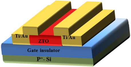
Figure 1 shows the schematic diagram of ZTO TFT structure. The ZTO film thickness was about 40 nm and patterned by using photolithography. The channel width and length are 250 μm and 50 μm, respectively. After deposition of the ZTO films, source and drain electrodes (Ti/Au=10 nm/50 nm) were fabricated by ebeam evaporation and lift off process. Then, annealing process was performed in different annealing conditions, such as air, wet and vacuum ambient. The ZTO TFT was annealed at 500℃ for 2 h. Air annealing treatment was performed in atmosphere condition, while wet annealing was performed in the ambient of heated de-ionized (DI) water. The amorphous structure of ZTO thin films was confirmed by X-ray diffraction (XRD). All electrical performance were measured by using a semiconductor parameter analyzer(EL 423).
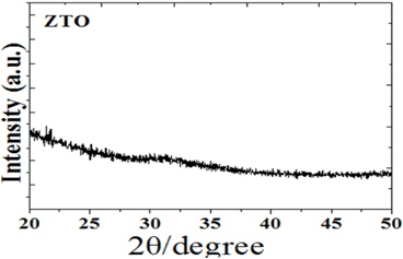
Figure 2 shows XRD patterns of ZTO thin films. The X-ray diffraction profiles for the films that are annealed at 500℃ exhibited amorphous structure [10,11].
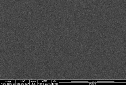
Figure 3 shows the surface microstructure of the ZTO thin films analyzed by SEM. In ZTO thin films, the surface is composed of small and uniform grains.
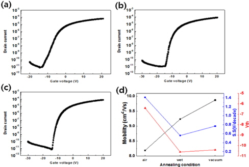
Figure 4 shows transfer characteristic of air, wet and vacuum annealed ZTO TFTs measured at VDS=5.1 V. Gate voltage (VGS) was swept from –30 V to 20 V. Transfer curve shows drain current of log plot (black line) and leakage current of linear plot (red line). We deduced threshold voltage (Vth) by extrapolation method in linear plot of drain current.
Table 1 shows the electrical performance of ZTO TFTs with different annealing condition. The field-effect mobility (μFE) was calculated by using the following relation: [12]
[Table 1.] The electrical performance of ZTO TFTs with different annealing condition.
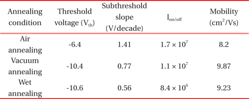
The electrical performance of ZTO TFTs with different annealing condition.
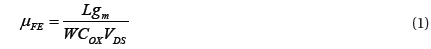
where, gm is the transconductance; Cox is the oxide capacitance of the gate insulator; W and L are channel width and length, respectively. In the case of air annealing, the threshold voltage (Vth), subthreshold slop (SS), drain current on/off ratio (Ion/off), and μFE were measured to be about –6.4 V, 1.41 V/decade, 1.7 × 10⁷ , and 8.2 cm2 /Vs, respectively. For the wet annealing, the Vth, SS, Ion/off, and the μFE were measured to be about –10.6 V, 0.56 V/decade, 1.1 × 10⁷ , and 9.23 cm2 /Vs, respectively. Also, in vacuum annealing, the Vth, SS, Ion/off, and the μFE were measured to be about –10.4 V, 0.77 V/decade, 8.4 × 10⁶ , and 9.87 cm2/Vs, respectively. Based on these results, it is interesting to note that wet and vacuum annealing treatment can improve the electrical characteristics of the device. It is understood by the generation of free electrons by adopting wet and vacuum annealing process. In the case of wet annealing, two possible mechanisms could be proposed to explain the performance improvement. One of the mechanisms is oxygen atoms of ZTO film reacting with neighboring hydrogen to generate H2O. This mechanism can be described as follows: [13]

where, Vo··an ionized oxygen vacancy, and e- denotes free electron. The second possibility is the carrier injection by the adsorption of H2O on the a-ZTO surface. H2O adsorption donates a partial negate charge to the channel surface with either molecules or hydroxyl forms [14]. In this case, the role of H2O could be defined as a donor. When the devices were annealed in vacuum, the oxygen in the channel would go through desorption from the device and induce more carrier concentration as well as density of states. On the other hand, air annealing treatment reduces the defective states such as oxygen vacancy [5]. It is understood by passivation effect of oxygen atoms.
Vacuum annealing process provides large amount of free electron, due to relatively less amount of oxygen in the furnace. Consequently, carrier concentration is increased by wet and vacuum annealing process.
In summary, we have fabricated the amorphous ZTO TFTs by solution process with different annealing conditions in the air, wet and vacuum ambient. XRD data shows the amorphous structure of ZTO thin films. The air annealing process reduces the sub-gap defective states, such as oxygen vacancy, and decreases the instability of the channel material. However, air annealing has suppressed the generation of free electron; hence, electrical performance was deteriorated. As a result, electrical characteristics such as field effect mobility and subthreshold swing were improved after wet and vacuum annealing treatment compared with air annealing treatment. Through this result, it is expected that wet and vacuum annealing process can improve device performance.