Since the discovery of new carbon allotropes in the second half of the 20th century, there has been considerable research into their production and applications. Zero-dimensional fullerene, which was discovered in 1985, carbon nanotubes, which were discovered in 1991, and two-dimensional graphene, which was the latest discovery, have been included in that research [1]. Graphene has a hexagonal lattice composed of carbon atoms with a one-atom thickness.
The Manchester group team and Geim first produced graphene by mechanical exfoliation using scotch tape in 2004 [2,3]. Graphene is very stable, both structurally and chemically, has a high electron mobility of 20,000 cm2/Vs and high thermal conductivity of 5,000 W/mK [4-6].
Graphene thin films can be obtained by using any one of four methods: mechanical exfoliation, chemical exfoliation, epitaxial growth, and chemical vapor deposition (CVD) [2,7-9]. The most common method is CVD, which involves the use of a catalytic metal such as Ni, Pd, Co, Cu or Au, and high temperatures of 1,000℃. In addition, a transfer process using a catalytic metal is required. The process is inefficient in terms of production costs, with many defects arising during the transfer process and further difficulties in mass production [10-12].
Pulsed laser deposition (PLD) is expected be an appropriate technique for thin film growth without any changes in the composition of the target, because ablation occurs momentarily when the target is irradiated with a laser beam. In addition, it is easy to produce crystalline carbon thin film materials, such as carbon nanostructures. One advantage of PLD is that transcription processes, which is a problem with CVD, can be eliminated, and a graphene thin film can be prepared without a catalytic metal. Graphene growth by PLD was confirmed to have a close relationship with temperature [13-15].
In this study, graphene thin films were grown on single crystal sapphire substrates without a catalytic metal, using pulsed laser deposition. The crystalline characteristics of grown graphene thin films were investigated.
A Quantel Brillant B Q-switched 4th harmonic Nd:YAG laser (λ= 266 nm) with a fluence maximum of 2 J/cm2 and a repetition rate of 10 Hz was used to deposit the graphene thin films by PLD. The laser power density was 1.2 J/cm2. The chamber for growth was initially evacuated to 10–5 Torr with an oil diffusion pump and a rotary pump.
The targets used to deposit thin films were highly ordered pyrolytic graphite (HOPG). The optical absorption rate of HOPG has a characteristic high optical absorption rate of the 4th harmonic (266 nm). The target was rotated at a constant speed of approximately 20 rpm so that the laser beam would irradiate different areas.
The substrates were located 40 mm away from the target at various temperatures between 400 and 600℃. A 1 cm × 1 cm × 0.4 mm sapphire substrate was used. The surfaces of the sapphire substrates were cleaned ultrasonically in acetone, ethanol and deionized water, for 10 minutes at each step, and then dried using an N2 gun. The cleaned sapphire substrates were then moved into a vacuum.
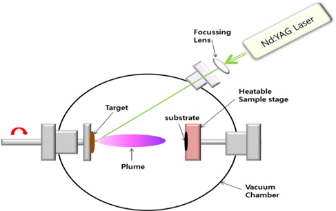
Figure 1 shows a schematic diagram of the PLD system used in this study. Table 1 lists the pulsed laser deposition conditions.
[Table 1.] Pulsed laser deposition conditions
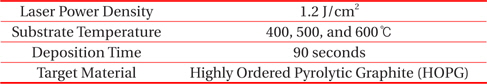
Pulsed laser deposition conditions
Raman spectroscopy with a green laser beam (514.2 nm) was used to examine the structure of graphene. The spectra were obtained in the range 1,000~3,000 cm–1. The surface topography of the graphene thin films was observed by atomic force microscopy (AFM). The chemical-bond state of the graphene thin films was analyzed by X-ray photoelectron spectroscopy (XPS).
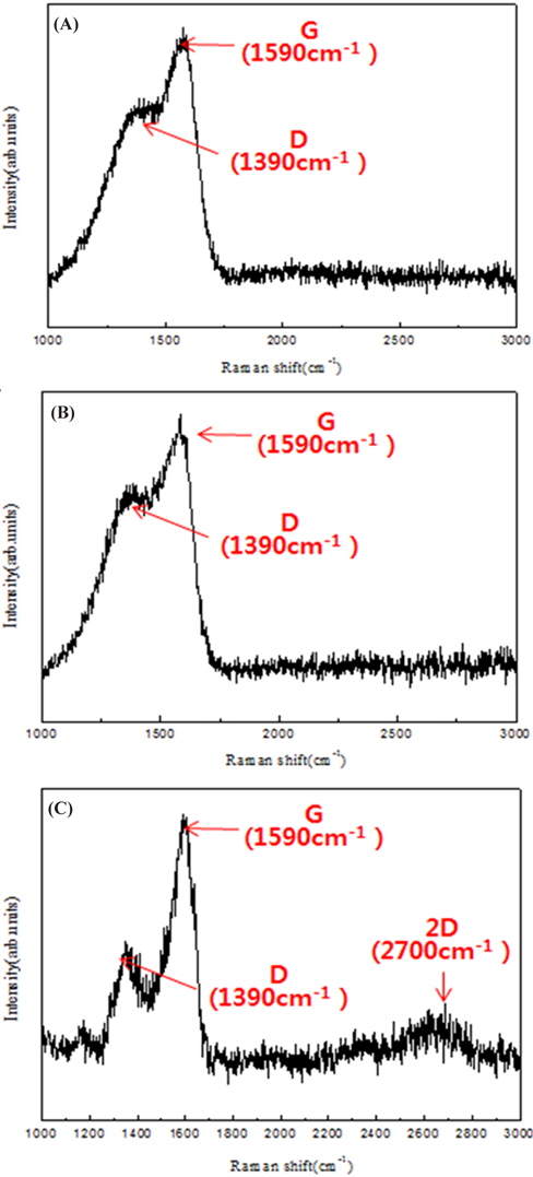
Figure 2 shows the Raman spectrum of the graphene thin film deposited with a 1.2 J/cm2 laser at a substrate temperature. The G band at 1,580 cm–1 was assigned to a non-resonant scattering process. The characteristics of the in-plane sp2 carbon hexagonal networks due to the optical phonon (E2g) near the Brillouin zone center (Γ point) were examined [16]. The presence of a G band is characteristic of the formation of a hexagonal carbon lattice.
The D band at 1,350 cm–1 and 2D band at 2,700 cm–1 were assigned to double resonant scattering processes. This involves two real spaces between two continuous electronic excitations with different energies and momenta, and is caused by phonons near the K point of the Brillouin zone. The D band indicates the disorder of the sp2 combined state. The 2D band will be present even in the absence of the D band. On the other hand, the 2D band to G band intensity ratio indicates the number of graphene layers [17].
Figures 2(A) and (B) show the 400℃ and 500℃ Raman spectra of the D peak and G peak spectra overlapping. This is a not crystallized form of graphene, which means that nano-graphite should be considered. Figure 2(C) shows that the 600℃ Raman spectra of the D peak and G peak were separated. The successful formation of graphene was considered. The ID/IG ratio of graphene formed at 600℃ was 0.55, which indicates the presence of defects in graphene. The I2D/IG ratio of the graphene formed at 600℃ was 0.3, which indicates three layers of graphene. Based on the peak in the Raman spectra, a few-layer graphene (FLG) sample was fabricated.
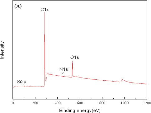
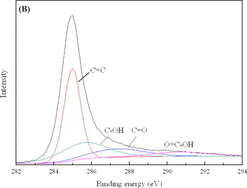
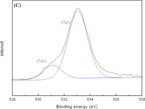
Figure 3(A) shows an XPS spectrum of the graphene thin film deposited with a laser density of 1.2 J/cm2 at a substrate temperature of 600℃. The XPS spectra survey indicated the range of binding energies from 0 to 1,200 eV, showing that the main chemical components are O1s, N1s, Si2p, and C1s. The component of the graphene thin film was C and O. Figure 3(B) shows an XPS spectrum of C1s. The C1s peak was observed as the main peak at 284 eV, which combines the binding states of the C=C, C-OH, C=O, and O=C-OH bonds. Figure 3(C) shows an XPS spectrum of O1s. The O1s peak shows the bonding state between oxygen and carbon. The main O1s peak was observed at 530 eV, which indicates the presence of C-O and C=O bonds. Based on the peak in the XPS spectra, the bond between the oxygen and carbon was considered.
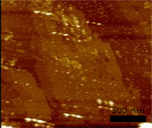
Figure 4 shows an AFM image of the graphene thin film deposited with a laser density of 1.2 J/cm2 at a substrate temperature of 600℃. The number of graphene layers was interpreted as FLG by Raman analysis, but the AFM image indicated three graphene layers.
To overcome the CVD growth method’s disadvantage of having to use a catalytic metal, graphene thin films were deposited directly without a catalytic metal by PLD, using a Nd:YAG laser. The formation of FLG at a substrate temperature of 600℃ was confirmed by Raman spectroscopy. On the other hand, nanographite was formed at substrate temperatures lower than 600℃. Nano-graphite formed in the graphene thin film with increasing substrate temperature. The formation of a graphene thin film was attributed to carbon particles being emitted from HOPG and rearranged by high substrate temperatures.