Germanium (Ge) has gained considerable interest for next generation nanoelectronics, due to its high mobility (its electron mobility is two times higher that of Si [1]). However, Ge n-channel metal-oxide-semiconductor field-effect transistors (MOSFETs) have been shown to have inferior drive current performance, compared to Si n-channel MOSFETs, which was attributed to electrically active defects on the Ge surfaces [2]. Another problem for realizing high performance Ge n-MOSFETs is the large effective Schottky barrier height at the metal/Ge interface, which results from the strong Fermi-level pinning [3]. It has been shown that the charge neutrality level (CNL) is located very close to the valence band edge EV of Ge [4], which eventually leads to a high contact resistance between metal/n-Ge contacts. In addition, this gives rise to the problem of the absence of Schottky barriers on p-type Ge [5]. As a result the investigation of electrical properties in Ge has mainly focused on n-type material [6]. Recently, concentrator photovoltaics (CPVs) based on In-GaP/(In)GaAs/Ge triple junction solar cells have been reported to achieve more than 30% efficiency [7]. In triple junction solar cells, p-type Ge wafer can be used as starting material, because it is easy to form p-n Ge bottom cells by diffusion of As or P atoms from the nucleation layer, such as GaAs or InGaP, during the overgrowth. To improve the cell efficiency, further understanding of p-type Ge layer with a high quality of metal contact is required.
Metal-semiconductor (MS) contacts are used to understand the carrier transport across the MS contacts, which are required to achieve high-performance Ge-based devices. Until now, several methods, such as In plating [8], passivation of the Ge surface [9,10], and insertion of a thin insulation layer [11,12], have been employed to obtain the metal/p-Ge Schottky contacts. Based on the results of hydrogen plasma treatment on p-type Ge, Kolkovsky et al. suggested that earlier difficulties in making good Schottky barriers were due to the presence of hydrogen acting as an acceptor in p-type Ge [5]. Thathachary et al. [9] reported on the fabrication of Zr and Al Schottky contacts by sulfur passivation of the Ga-doped Ge surface. The barrier heights for the metals were evaluated as 0.6 and 0.57 eV for Zr and Al, respectively. Using Se treatment, Janardhanam et al. obtained a barrier height of 0.33 eV for Al/p-Ge Schottky contact [10]. Nishimura et al. showed that by inserting a very thin oxide layer, such as GeOx or AlOx, Al and Au metal contacts to p-Ge can be changed from ohmic to rectifying characteristics, by varying the thickness of the oxide layer [11].
Among contact metals, Cu possesses excellent electrical and thermal conductivities. It is well known that Cu is prone to diffuse into Si semiconductor, without any diffusion barrier [13]. The failure mechanism and indiffusion parameters for Cu contacts with the InGaP layer have also been demonstrated [14]. These indicate that Cu atoms can diffuse into a Ge layer. Thus, detailed studies of the interface characteristics between Cu and Ge layers are very important for achieving high performance in Ge-based devices. To the best of our knowledge, however, there is little knowledge concerning the Cu Schottky contacts with p-type Ge. This work conducted electrical characterization of Cu/p-type Ge Schottky contacts, to understand the current transport mechanism across the Cu/p-Ge interface.
Ga-doped Ge (100) wafers (thickness: 500 μm, size: 2 inch) were used in this investigation. Single side polished Ge wafer, grown by the Czochralski method, was purchased from i-Nexus Inc. The room-temperature carrier concentration was about ~1 × 1017cm−3. These samples were cut into small pieces. Copper (Cu) Schottky contacts with a thickness of 50 nm were deposited by radio-frequency (RF) magnetron sputtering through a shadow mask onto the Ge surface, after solvent cleaning. For Ohmic contact, In metal was rubbed over approximately half of the sample. Current-voltage (I-V) measurements were performed at room temperature, using an HP 4155C semiconductor parameter analyzer.
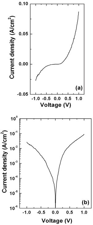
Figure 1 shows the (a) linear, and (b) semilogarithmic I-V characteristics measured at room temperature. The forward bias characteristics of a Schottky diode based on the thermionic emission (TE) model are given by [15]:


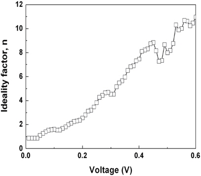
where, I0 is the reverse bias saturation current, A is the diode area, A** is the effective Richardson constant (48 Acm−2K−2 for p-type Ge [11]), ΦB is the effective Schottky barrier height, n is the ideality factor, V is the applied voltage, and RS is the series resistance. For values of V greater than 3 kT/q, the ideality factor can be obtained from the slope of the linear region of the ln(I)-V curves. The forward I-V analyses revealed that ΦB = 0.66 eV and n = 1.92. The ideality factor at room temperature was larger than unity, which has been attributed to the presence of interfacial states and an insulator layer between the metal and the semiconductor [16]. The bias-voltage-dependent ideality factor n(V) could be obtained through the relation of
The corresponding curve in Fig. 2 shows that the ideality factor increases slowly with increasing forward bias in the region where the effect of the series resistance is small (e.g. linear region of ln(I)-V), and then increases more rapidly with increasing forward bias, where the effect of the series resistance dominates the ln(I)-V characteristics. The latter effect gives rise to the curvature at higher current in the semilogarithmic I-V plot, as Fig. 1(b) shows.
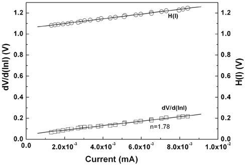
The series resistance (RS), an important parameter in the electrical characteristics of Schottky barrier diodes, results from contact wires, or from the bulk resistance of the semiconductor, the interfacial layer, and the interface states. According to Cheung’s model, the values of series resistance can be determined from the slopes of the following equations [17]:


where, H(I) is given by
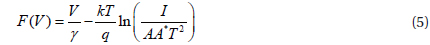
Norde proposed an empirical function to calculate both the barrier height and series resistance for a Schottky diode [18]. The Norde function is defined as:

where,

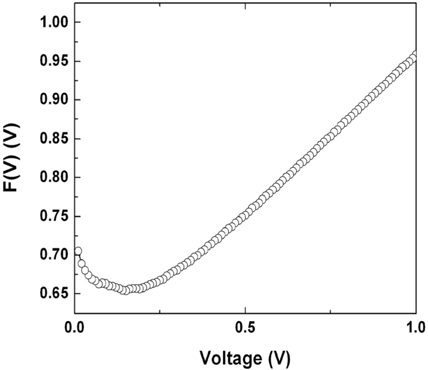
where, F(Vmin) is the minimum value of F(V), and Vmin is the corresponding voltage. Figure 4 shows the F(V)-V curve of the Cu/p-Ge Schottky diode. The barrier height obtained was 0.70 eV. The barrier height obtained from the Norde method is a little higher than those from the forward bias ln(I)-V and Cheung methods. Such differences in the barrier height values could be attributed to the extraction from different regions of the forwardbias I-V plot. In other words, forward ln(I)-V and Cheung methods are applied to the linear (low voltage) and non-linear (high voltage) sections of the forward-bias ln(I)-V characteristics, respectively. On the other hand, the Norde method is applied to the full forward-bias region of the ln(I)-V characteristics of the junctions [6].
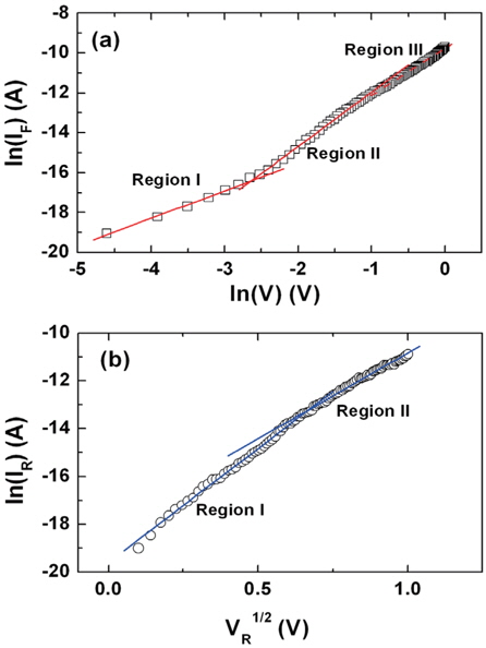
As Fig. 5 (a) shows, the forward-bias ln(I)-ln(V) curve is characterized by three linear regions, indicating different conduction mechanisms. At low voltages (Region I), an ohmic conduction is dominant where the logarithmic slope is about 1.4. In this region, the injection of charge carriers from the electrodes into the semiconductor material is considerably reduced, due to the low bias voltage, and tunneling is the dominant current transport mechanism. In Region II, a square law region appears with a slope of 2.7, and charge transport is mainly governed by the space charge limited current (SCLC), with an exponential distribution of traps in the band gap [19]. At high voltages (Region III), the slope decreases to about 2.3, indicating that the device approaches trap-free SCLC [6]).
As shown in Fig. 5(b), the reverse-biased current transport was analyzed using the form of ln(I) vs. V1/2. The linearity in the curve can be interpreted via either the Schottky effect, or the Poole-Frenkel effect. Current-voltage expressions are given as [20]:
for the Schottky effect, and as:
for the Poole-Frenkel effect. Here, J0 (= σ0F, where σ0 is the low-field conductivity, which depends on the carrier mobility and the donor activation energy) is the low-field current density. βS and βPF are, respectively, the Schottky and the Poole-Frenkel field lowering coefficients given by 2
For the Cu/p-Ge Schottky contact, we observed two regions of linear variation with a slope of 9.60 × 10⁻⁵ eV m1/2V−1/2 in the lower bias region (Region I), and 7.20 × 10⁻⁵ eV m1/2V−1/2 in the higher bias region (Region II). A comparison of the experimental and theoretical slopes revealed that the experimental slopes for both in the low and high bias regions were much closer to those of the Poole-Frenkel effect. In Schottky emission, the carrier that absorbs the thermal energy emits over the potential barrier at the interface; whereas in Poole-Frenkel emission, the carrier transport occurs through trap states, by applying an electric field [22]. Furthermore, Kobayashi et al. observed a very large ideality factor in the thicker SiN region for the Al/SiN/n-Ge Schottky diode, which they explained by the transport mechanism due to the tunneling and/or the Poole-Frenkel emission [23]. Based on the results so far, we can deduce that the effect of the presence of an interfacial layer and interface states is significant on the current transport in the Cu/p-Ge Schottky diode. Further investigation employing various surface treatments on p-type Ge is underway.
We performed current-voltage (I-V) measurements, to characterize the electrical properties in Cu/p-type Ge Schottky contacts. We obtained Schottky barrier heights of 0.66, 0.59, and 0.70 eV from the forward ln(I)-V, Cheung, and Norde methods, respectively. We obtained the ideality factors of 1.92 and 1.78 from the forward ln(I)-V and Cheung methods, respectively. A higher ideality factor than unity would be due to the presence of an interfacial layer and interface states across the Cu/p-Ge interface. The reverse-biased current transport was more closely related to the Poole-Frenkel effect, than to the Schottky effect.