Recently, the application of infrared optical systems in hightech industries such as in infrared CCTV cameras, aerospace satellites and medical optical systems have started to see a gradual expansion [1,2]. In the medical field, a thermographic diagnostic technique which measures the distribution of body temperature without contact is widely being used as special equipment for measuring changes in local temperature during various procedures. In addition, research on video implementation for small-sized medical instruments is also being carried out using thermal infrared. Subsequent interest in infrared optical systems has necessitated the promotion of the performance and productivity of optical systems, and the reduction of production costs. Currently, glass materials in the Chalcogenide system are receiving attention in the production of infrared optical systems [3,4]. Chalcogenide materials have high optical transmission of infrared rays and can be produced by high temperature compression molding using a molding core [5]. However, such high temperature compression molding has a number of shortfalls including chemical changes in the dependent characteristics of the glass material and molding, as well as decline of the life span caused by deformity due to the high temperature and pressure.
The change in shape caused by the chemical changes on the contacting surface, and high temperature and pressure depends on the characteristics of the glass materials and the molding conditions. In order to solve the associated problems, it is necessary to develop coating techniques for molding the surface of the tungsten carbide. DLC coating, which has been studied in a number of fields, is characterized by extreme hardness, high elasticity, abrasion resistance and chemical stability [6-10]. Demon-strating diamond-like properties, DLC can be produced through various methods, such as ion beam puttering [11], ECR CVD (Electron cyclotron Resonance Chemical Vapor Deposition) [12], PECVD (Plasma Enhanced Chemical Vapor Deposition) [13], laser ablation [14], and FVAS (Filtered Vacuum Arc Source) [15,16], and has high industrial application. In the present study, a DLC thin film was deposited on a cemented carbide used as the material of the molding core for application to the production of medical thermal infrared lenses, and the resulting characteristics were analyzed.
DLC thin films can be manufactured in a number of ways, including ion beam sputtering, chemical vapor deposition and laser ablation. DLC thin films have excellent mechanical properties and chemical stability, and a high level of optical transparency [17]. However, they also have the weakness of low adhesion to metal materials and oxidization at low temperatures, since they contain hydrogen. Therefore, a filtered arc system was used herein to deposit a high quality DLC thin film onto tungsten carbide used for a high temperature compression molding core.
The filtered arc system used in the present study can prevent the hydrogen from being incorporated into the thin film by using solid graphite, not the hydrocarbon gas used in physical deposition [18,19]. Therefore, it is possible to deposit a DLC thin film with extreme harness and density like diamond, high adhesion between the substrate and the thin film, high optical properties, and high thermal stability, depending on the possibility of depositing a high quality thin film which does not containing hydrogen and has high ion energy and flux [20].
The filtered arc system generates carbon ions on the carbon substrate using a strong arc discharge, and can convey them to the substrate for deposition through its strong magnetic field. In addition, it can produce a flat thin film by employing a separate magnetic filter tube in order to remove the macro particles often produced by the arc source [21]. Changing the substrate bias voltage to -100 V, -150 V, and -200 V, the DLC thin film was deposited onto the silicon wafer and tungsten carbide for mechanical analysis and comparative analysis of the optical properties.
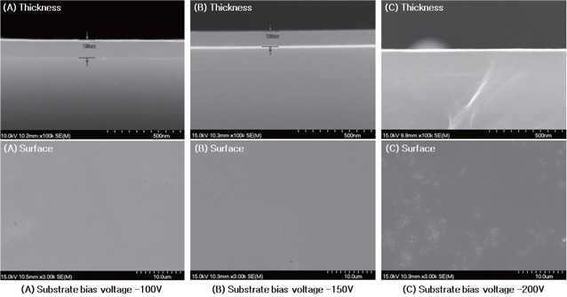
To analyze the surface and thickness of the DLC thin film generated by each processing condition, the surface and cross section were examined via SEM (S-4700, Hitachi, Japan) after deposition of the DLC thin film onto the silicon substrate. Figure 1 shows the surface and thickness of the thin film for each processing condition.
It was found that the thickness of the thin film was reduced to 123 nm with an increase in the substrate bias voltage from -100 V and 105 nm to -150 V.
Moreover, when the substrate bias voltage was -200 V, measurement was not possible because the boundary between the thin film and the plate could not be distinguished. Regarding the surface of the thin film, a relatively uniform deposition surface could be observed when the substrate bias voltages of -100 V and -150 V were used, while the deposition surface was not even with the substrate bias voltage of -200 V.
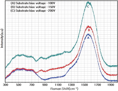
Raman analysis is well known as a useful method of analyzing the structure of amorphous materials such as DLC.
DLC is a carbon thin film with a combination of mixed amorphous structures such as sp3 (diamond-liked or tetrahedral bond), sp2 (graphite-like or trigonal bond) and sp1 (hybridization C-C bond). Graphite and diamond, with carbon as their main components, are in a crystalline state consisting completely of sp2 and sp3 carbons, respectively [22]. However, the properties of a DLC thin film, an amorphous material, differ depending on the fraction of sp3/sp2 inside the carbon-carbon coupling [23,24].
Raman spectroscopy was conducted herein in order to determine the state of the combination of the DLC thin film generated under each processing condition. A LabRam HR-800 was used in analysis, measuring the range of 300~2,000 cm−1 using a 514 nm Ar+ ion Laser. The results of the measurements of each processing condition are shown in Fig. 2.
Unlike other deposition methods, the filtered arc system employed in this study used no hydrogen component in the sample and the process environment, allowing the formation of a non-hydrogenated amorphous carbon thin film with excellent mechanical properties [25]. The combining state of DLC film is analyzed based on the G position and the sp2 distribution in manufacturing the DLC thin film, wherein ta-c with less sp2 component is proposed when the position of G peak is 1,560~70 cm−1 [6,26].
Analysis of the G peak in each process condition revealed that the G peak was located at 1,561 cm−1 for almost all of the processing conditions. Therefore, it was judged that ta-c thin film with a high sp3 fraction was formed.
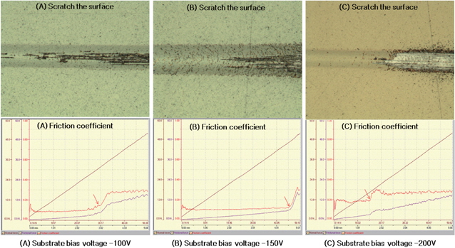
Thin film deposition is a bonding process between different foreign substances, all of which have different properties. The difference in properties causes differences in the bond strength between a thin film and a substrate [27]. Therefore, a scratch test was carried out on the DLC thin film deposited on tungsten carbide at each processing condition herein, for use as a substrate for a molding core. A scratch was generated on the surface of the specimen while increasing the load regularly using a stylus with a certain shape, and the load when the DLC thin film began to separate from the tungsten carbide was measured. The results of the scratch test are shown in Fig. 3. The top images show the DLC coating surface of the tungsten carbide with a scratch, While the bottom images show the change in friction coefficient and friction according to change of the load and stylus.
For the scratch test (Revetest, CSEM, Switzerland) carried out herein, the initial load was set to 1.3~4 N, which was then increased by 10N per minute, and a force of up to 50 N was added. The critical load, the basis of the adhesion between the tungsten carbide and the DLC thin film, was measured by converting the point in time when a fine scratch was generated based on the micrograph image to distance. The critical load of 21.3 N was observed when the bias voltage of the substrate was -100 V, 38.6 N when it was -150 V, and 16.36 N when it was -200 V. The adhesion of the thin film was found to be the highest at 38.6 N, when the bias voltage of the substrate was -150 V. When the bias voltage was -200 V, a phenomenon of the separation of the thin film appeared rather than fine irregularities.
3.4 Surface analysis (Tungsten carbide)
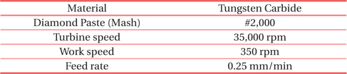
The surface shape and roughness of the surface of the molding core used in molding makes a big difference in the optical properties of a glass lens. To analyze the impact on the roughness of the DLC thin film, the surface of the tungsten carbide used for an actual molding core was ground and the PV (peak to value) and Ra (roughness) of the surface were measured before and after deposition of the thin film. A polishing machine (KRP-2200F, Kurda Co., Japan ) was used to grind the surface of the tungsten carbide, and wet processing was carried out using diamond paste. Table 1 shows the grinding conditions.
[Table 1.] The grinding conditions of tungsten carbide material.

The grinding conditions of tungsten carbide material.
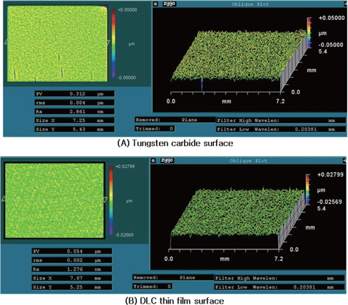
To check the changes in the PV and Ra of the surface due to coating of the DLC thin film, a 3D surface roughness measuring instrument (NewView 5000, Zygo, USA) was used. To check the surface of the tungsten carbide used, grinding work was carried out and then a DLC thin film was deposited with the bias voltage of -150 V. For measurement before and after the deposition on tungsten carbide, 2.5x was used for the 3D surface roughness measuring instrument. From the center of the surface of the measurement, the X-axis of approximately 7 mm and Y-axis of approximately 5 mm were measured. The results are shown in Fig. 4.
The PV of the ground tungsten carbide before coating was found to be 0.312 um, and the Ra of the surface was 2.861 nm. After the coating of the DLC thin film, the PV was 0.054 um and the Ra of the surface was 1.276 nm. The PV showed a rapid change from 0.312 to 0.054 um after coating, and the deposition thickness of the DLC thin film at the substrate bias voltage of -150 V was 100 nm, caused by bumps remaining in the polished surface of the tungsten carbide. However, the Ra of the surface changed from 2.861 nm before deposition to 1.276 nm after deposition. From this result, it was judged that a flat deposition was made without the generation of macro particles in the filtered arc system used, allowing improvement of the Ra of the surface by the deposition of the DLC thin film.
To perform basic research on the improvement in the performance of the molding core used in infrared optical system production, DLC thin film was deposited onto a tungsten carbide substrate with different bias voltages and the characteristics were analyzed. A filtered arc system was used for the deposition of the DLC thin film while changing the process conditions with a substrate bias voltage of -100 V, -150 V, and -200 V on the tungsten carbide used for the silicon wafer and the molding core. Through SEM analysis, it was found that the DLC thin film deposited became thinner with each change of the bias voltage of the substrate from -100 V to -200 V, and that the surface was relatively uniform when the bias voltages of -100 V and -150 V were used. After deposition of the DLC thin film with the processing conditions of the bias voltage of -100 V, -150 V and -200 V on the tungsten carbide used as a substrate of a molding core, Raman analysis was carried out in order to examine the components of the deposited thin film. The G peak was found at approximately 1,561 cm−1 in the thin films deposited under each condition. Based on this observation, it was judged that a ta-c thin film with high sp3 fraction was formed. A scratch test to check the adhesion between the DLC thin film and the tungsten carbide showed the strongest bonding at the bias voltage of -150 V. To verify the improvement of the surface by deposition of the DLC thin film, comparative analysis was carried out before and after the deposition. Consequently, the Ra was improved by the deposition of the DLC thin film, through which it was judged that the production of a superior lens may be possible.