It is well known that organic light emitting diodes (OLEDs) are attracting great interest in the display technology industry due to their many advantages, such as their low price of manufacturing, large-area of electroluminescent display, and various colors of emission including white light [1].
Recently, there has been much progress in understanding the device physics of OLEDs and their basic operating principles [2].
In LEDs, light emission is the result of the recombination of the electron and the hole in the light- emitting layer. The electron and the hole are injected from cathode and anode. To improve the efficiency of luminescence, the hole and electron pairs need to exist in abundance and equally, and recombine swiftly in the emitting layer [3,4].
In order to understand the operation of an OLED, it is needed to study the injection, transport, and recombination processes involved in the physical phenomenon. There have been extensive studies of charge injection and transport for the single layer and single carrier devices [2].
At low voltage, the mobility is independent of the electric field, but this is not the case at high voltage.
Conduction in the organic light emitting diodes (OLED) strongly depends on the carrier mobility (the carrier mobility of injected electrons and holes are different), and the injection barrier between the electrodes and the organic layer. The height of the injection barrier determines the mode of conduction in an OLED. It is limited by the volume: one of the two contacts electrode / organic must be Ohmic (follow Ohmic Law at low voltage or SCLC (current limited by the space charge) and TCL (trap current limited) laws at higher voltage), or limited by the injection (described by Fowler Nordheim model for tunneling injection, or by the Schottky Richardson model for thermionic emission) [7].
In this paper, two structures have been investigated using ATLAS -SIVACO software. The first structure was realized using a polymer poly (2-methoxy,5-(2’-ethyl-hexoxy)-1,4-phenylenevinylene)] MEH-PPV as an active layer. In the second structure we use small molecule tris (8-hydroxyquinolinato) aluminum (Alq3) as both the electron transport material (ETM) and emitter layer.
We choose MEH-PPV because of its solubility in common organic solvents, in conjunction with a low operating voltage for light emission and relatively high conversion efficiency and Alq3, which is one of the most important host materials used in OLEDs.
2. MODELS AND DEVICE PARAMETERS
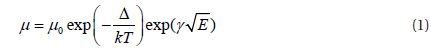
In organic polymer LED simulation, the Poole-Frenkel like mobility model and the Langevin bimolecular recombination model have been used as the transport and recombination mechanism.
In addition, to infer the radiative rates for luminescence or phosphorescence due to the Langevin recombination in organic LEDs, the distribution of singlet or triplet excitons has to be calculated. For the Poole-Frenkel-like mobility model, additional parameters such as, the thermal activation energy of the organic polymer at zero electric field for electrons and holes, and the electron and hole Poole-Frenkel factor are specified in the MOBILITY statement [6].
When the applied electric field is large, carrier mobility is not constant, and depends on the temperature and the applied field, and one of the ways to introduce the field effect is to use the Poole-Frenkel effect.

To receive maximum quantum efficiency, it is assumed that all carriers are recombined.
First, the electric field has to be calculated from the change of charge density.

In order to obtain the recombination ratio, the current continuity equation must be solved.


Where n and p are concentrations of the electron and hole, respectively. -G and R are generation and recombination ratios.
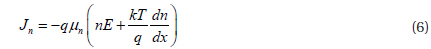
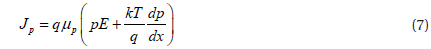
Here, the mobilities of the electron and the hole in OLED are related to the time dependent continuity equation, drift - diffusion relation and Poisson's equation. [10,11].


Where Jn and Jp are electron and hole current densities, μn and μp are electron and hole mobility, ε is organic dielectric constant, k is Boltzmann constant, T is temperature.
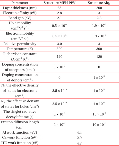
The simulation parameters of PLED ITO/MEH-PPV/Al (Ca)) and (ITO/Alq3/Ca) implemented in the ATLAS -SILVACO code are presented in Table 1. [6,9].
[Table 1.] Simulation parameters.

Simulation parameters.
Device simulation structure
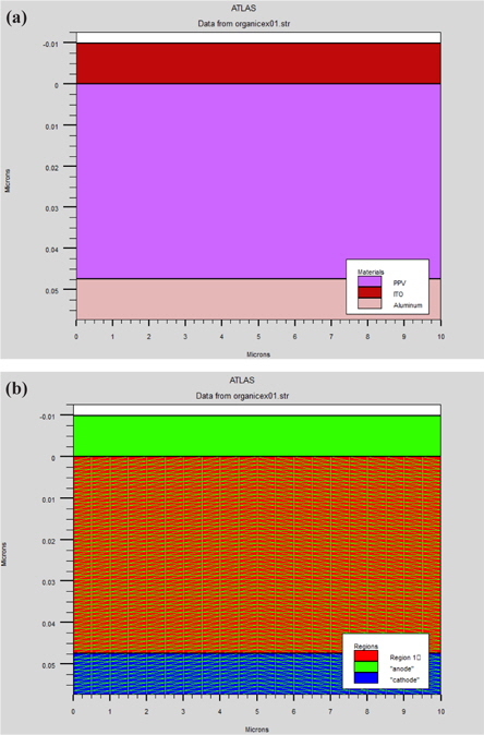
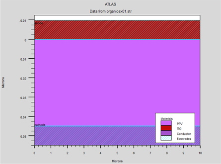
The PLED simulation structure used in this paper is a mono layer device; typically consisting of the poly(2-methoxy-5(2’-ethyl) hexoxy-phenylenevinylene) (MEH-PPV) polymer sandwiched between an anode with a high work function, usually an indium tin oxide (ITO) substrate, and a cathode with a relatively low work function, such as Al, Ca deposited by vacuum evaporation. Electrons are then injected from the cathode and recombine with electron holes injected from the anode, emitting light. This is shown in Fig. 1.
In the case of MEH-PPV, the injection of carriers is determined by the height of barriers: electrodes - polymer. For this, PLEDs were performed with favored injection holes or electrons. This effect is obtained by adjusting the gap between the work function of the cathode metal and the electron affinity of the polymer on the one hand, and between the work function of the metal of the anode and the energy of ionization of the polymer, on the other hand. Thus, interfaces - metal - polymer- may either promote passage holes or electrons.
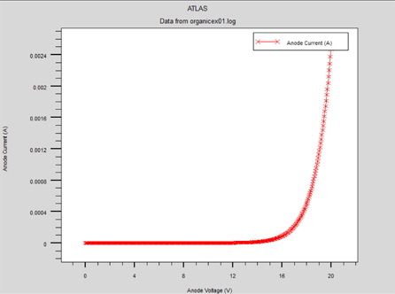
The "hole-only" device can be obtained by using a high work function metal, such as Al (4.4 eV), at the cathode. The use of high work function metal contributes a high energy offset between the Fermi energy at the cathode and the LUMO level in the MEH-PPV (which is 2.8 eV). This effectively reduces the number of injected electrons at the cathode and, therefore, the injected holes at the anode dominate [6]. This structure supports the single injection of holes. In this structure, the current follows the SCL law indicating that the volume limits the hole current and when the electric field increases, the mobility follows the Poole-Frenkel-like mobility model. [5]
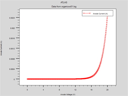
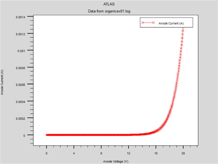
Figure 2 shows the electrical characteristics of the "hole-only" ITO/MEH-PPV/Al device.
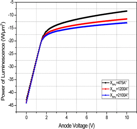
On the other hand, Figure 3 shows the electrical characteristics of the "hole-only" ITO/MEH-PPV/Al device by varying its polymer thickness. The simulated luminescence versus the applied voltage of the "hole only" polymer device with different polymer thickness ranging from 475 Å to 2,100 Å is shown in Fig. 4. A similar analysis was carried out for the "electron only" devices. Here, the ITO at the anode contact is replaced with a lower work function metal such as Ca (2.9 ev). Due to the large energy offset between the Fermi level of the anode and the HOMO of the MEH-PPV, the number of injected holes decreases. As such, most of the carriers in such devices are almost dominated by electrons [6].
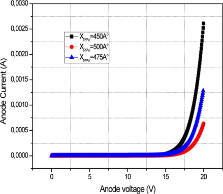
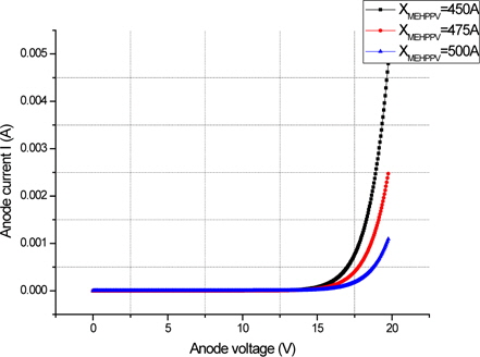
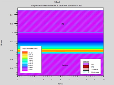
Figure 6 shows a plot of the simulated current versus anode voltage for an "electron-only" Ca/MEH-PPV/Ca device with varying polymer thickness of 450 Å, 475 Å, and 500 Å. With this second structure, which can inject electrons, the current is low. This current, limited by the traps, strongly depends on the electric field and follows the TCL law with traps exponentially distributed. Due to generally low charge carrier mobility in organic solids, the recombination zone is usually located at one of the contacts. (Fig. 7).
Finally, we will study the electrical characteristics of the twocarriers ITO/MEH-PPV/Ca OLED device (Fig. 8). The I-V characteristics show a small difference between the single injection of holes and double injection.
Device simulation structure
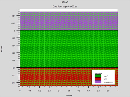
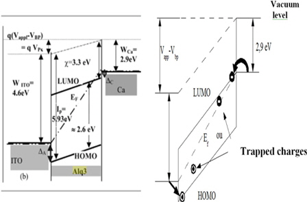
In this structure, we replace the poly(2-methoxy-5(2’-ethyl) hexoxy-phenylenevinylene) (MEH-PPV) by tris(8-hydroxyquinolinato) aluminum (Alq3) (Fig. 10). This simplified structure can be useful to study the transport properties and injection properties. Here, we discuss the first point that we can review for the choice of the cathode electrode in calcium. We can see, in Fig. 11, that the calcium work function (2.9 eV) is very close to the electron affinity of Alq3 (3 eV), which gives an absolute difference of 0.1 eV.
Therefore, the injection of electrons from the cathode should be relatively easily.
By contrast, the energy barrier between the ITO (4.7eV) and the HOMO of Alq3 (5.8 eV) is large, of the order of 1.1 eV, which means that the holes are hardly created within the device. When the applied voltage is sufficient to incline bands, the holes will be generated by tunnel effect. This will limit the generation of excitons and, therefore, the emission of photons.
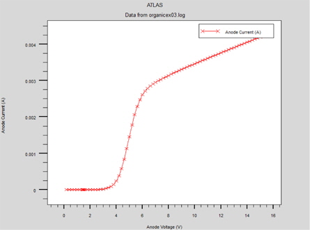
After reaching the potential of flat bands, the device turns on for electrons and an Ohmic regime is established (Fig. 11).
Starting from an applied voltage of about 5 V, two mechanisms appear: holes begin to be injected by the tunnel effect, and the charges are trapped and the current becomes limited by the traps. For an applied voltage of about 5.5 V, all the traps are filled and we can see that the hole injection is always carried out by the tunnel effect.
Consequently, the charge recombination is possible and the light is emitted. In addition, for higher voltages, the conduction is no longer limited by charge injection but by the space charge created by the trapped charges [8]. (Fig. 12).
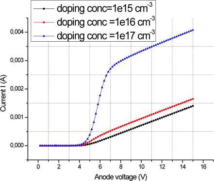
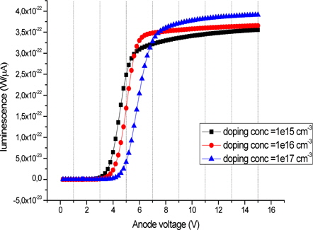
Figure 13 shows the electrical characteristics of an ITO/Alq3/ Ca device by varying its doping.
The simulated luminescence versus the applied voltage of OLED with different polymer doping ranging from 1 × 10¹⁵ to 1 × 1017 cm3 is shown in Fig. 14. The injection of holes within the device is more difficult than the injection of electrons; it can be done from a value close to the operating voltage, so that electrons and holes recombine.
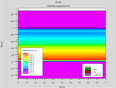
Moreover, in this type of device the generation of excitons must be very close to the interface between the ITO and Alq3 (Fig. 15).
This paper presents, a study of optical (luminescence) and electrical properties (I-V characteristic) of PLED based on MEHPPV and OLED based on small molecules Alq3.
The influence of parameters, such as thickness and doping, on I-V characteristics and luminescence are investigated. For the single layer devices, we observed that the luminescence and the current increased with the doping concentration and decreased with the thickness.
The analysis of these characteristics, I-L-V, shows us the complexity of injection mechanisms, since we observed several distinct phenomena related to the injection of charges, and to their transport within the devices. In summary, we can say that the injection of charges can occur through the thermionic and tunneling effect, and the conduction is limited by the space charge.
Due to the generally low charge carrier mobility in organic solids, the recombination zone is usually located at one of the contacts, depending on which mobility is limiting.
This is not ideal because the emitted light will be quenched more easily by the contacts. Therefore, it is necessary to add layers to enhance the injected charge (electrons and holes).
In terms of the choice of electrode materials, it is assumed that the diodes are optimized when the work function of the anode is equal to the ionization potential of the organic semiconductor and the cathode work function is equal to the electron affinity of the organic semiconductor.


![Diagram band of ITO/Alq3/Ca [8].](http://oak.go.kr/repository/journal/15578/E1TEAO_2015_v16n3_124_f011.jpg)