Amorphous oxide thin film transistors (TFTs) | have advantages of high mobility and low temperature in device fabrication. Since they also have high transparency in the visible range, they were regarded as transparent TFTs (TTFTs) [1-3]. Amorphous InGaZnO (a-IGZO) is regarded as channel layer of TTFT due their good performance, transparency, and stability [4]. There are many studies of channel layer as well as source and drain (S/ D) electrodes of TTFTs, because the S/D electrodes have an effect on the electrical performance and transparency of TTFTs. Transparent conductive oxides (TCOs) are suitable for the S/D electrodes of TTFTs due to their high optical bandgap (> 3.5 eV), good electrical conductivity, and high optical transparency of 80% in visible-infrared. Particularly, amorphous indium zinc oxide (a-IZO) was used for S/D electrode of ZnO TTFTs, due to high transparency and lower resistivity. Although there have been many researches on S/D electrodes of ZnO based TFTs, regarding their transparency, resistivity, and contact problem with channel layer, the relationship between the stability of ZnO based TFTs under the various stress and S/D electrodes is still unknown [5-8].
In this paper, the influence of S/D electrodes on contact resistance of a-IGZO TFTs has been investigated by transmission line method (TLM). The change in S/D electrode has an effect on interfacial traps and energy barrier between the channel layer and S/D electrodes. The different contact resistance in electrical performance of a-IGZO TFTs, depending on S/D electrode, has been studied using TLM. .
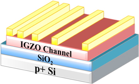
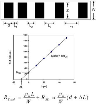
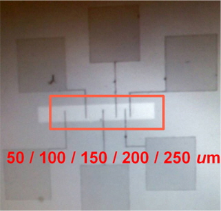
The a-IGZO TFTs were fabricated by using a thermally grown SiO2 thin film on highly p-type Si (001) substrate as both substrate and gate electrode. The a-IGZO layer (50 nm) was deposited using rf magnetron sputtering with the channel width (250 μm) and channel length (Lch) ranging from 100 μm to 650 μm, as shown in Fig. 1. All devices were annealed at 350℃ for 1 h in N2 ambient. Then, the different electrode was deposited and patterned using lift-off method. The Ti (10 nm) and Au (60 nm) as S/D electrodes was deposited by e-beam and thermal evaporation, respectively. The a-IZO electrodes and a-IGZO layer of a-IGZO/Ag/a-IGZO electrodes were grown by rf magnetron sputter method, and the Ag was deposited using the thermal evaporation. Figure 2 shows optical microscope image of real TLM patterned devices. Transfer characteristics are measured at a drain voltage VDS of 5.1 V with a single-sweep gate voltage VGS mode from -20 to 40 V. The Vth is defined as the VGS value, where a drain current IDS of 5 nA flows.
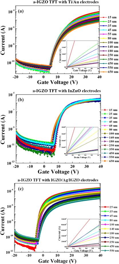
Figure 3 shows the transfer curves of a-IGZO TFTs depending on Lch with (a) Ti /Au electrodes, (b) a-IZO electrodes, and (c) aIGZO/ Ag/ a-IGZO electrodes. The inset shows output characteristics of a-IGZO TFTs measured at VGS = 15 V with different Lchs. As Lch increases, the off current (Ioff) and subthreshold swing (SS) were increased and the on current (Ion) was decreased, since the resistivity of channel and total trap density were increased. It is observed that the electrical properties of a-IGZO TFTs were different depending on the contact between the a-IGZO and S/D electrode. In the case of the device with Ti/Au electrode, the on current was higher but the value of SS was also higher than those of a-IZO electrode. However, the a-IGZO TFT with Oxide/Metal/Oxide (OMO) electrode showed good performance in both respects.
In order to investigate the specific contact resistance with various electrodes, the transfer line method (TLM) was used. Total resistance (Rtot) was determined from the slope of the linear region of the output characteristics by using Equation (1) [9,10].

where Lch is the separation of the electrodes, and W is the electrode width fixed at 250 μm, as shown in Fig. 4. Rtot is a function of the contact resistances (RSD) of the two contacts and the sheet resistance (RSH) of the semiconducting layer outside the contact, and RSD and RSH were obtained from the y-axis intercept and slope the Rtot - Lch plot of Fig. 5, respectively.
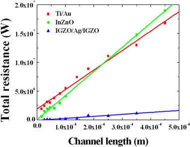
Figure 5 shows total resistance variation as a function of channel length depending on various electrodes. The RSD with Ti /Au was higher than that with the a-IZO, and IGZO/Ag/IGZO electrodes and the ratio of RSD /RSH were also higher. This is mainly due to low energy barrier between the channel and S/D electrodes, so the oxide electrodes were easy for injecting the carriers into channel layer. Therefore, the IGZO/Ag/IGZO electrodes showed low contact resistance for S/D electrodes of a-IGZO TFTs.
In conclusion, different S/D electrodes of the a-IGZO TFTs have been compared by TLM. The electrical properties and stability of a-IGZO TFT showed a different trend with S/D electrodes. The a-IGZO TFTs with a-IGZO/Ag/a-IGZO of S/D electrodes had a good performance and a low contact resistance due to the homo-junction with channel layer. It is clearly observed that the RSD with Ti /Au was higher than that with the a-IZO and IGZO/Ag/IGZO electrodes, and the ratio of RSD /RSH was also higher. This is mainly due to low energy barrier between the channel and S/D electrodes, so the oxide electrodes were easy for injecting the carriers into channel layer. Therefore, the IGZO/Ag/IGZO electrodes showed low contact resistance for S/D electrodes of a-IGZO TFTs.