Transparent conducting oxides (TCOs) are special semiconductors that possess three physical properties: high optical transparency, low reflectivity, and high electrical conductivity [1-4]. They are used as transparent conducting coatings, and have been widely used in a variety of electronic and optoelectronic device applications [5-11] such as organic light emitting diodes (OLED), liquid crystal displays (LCD), solar cells [12-17], and anti-reflection casting. To date, a number of research projects have been successfully carried out in the area of TCO materials. Important TCO semiconductors include impurity-doped ZnO, In2O3, SnO2, and CdO, ternary compounds including Zn2SnO4, ZnSnO3, Zn2In2O5, Zn3In2O6, In2SnO4, and CdSnO3, as well as multi-component oxides consisting of combinations of ZnO, In2O3, and SnO2. However, among many TCO materials, Sn doped In2O3 (ITO) is still the preferred material for most present applications. ITO has a multitude of properties, including degenerated semiconductor (n-type) behavior with a controllable resistivity and high optical gap (3.6eV) [18,19]. The low resistivity of ITO film is believed to be due to the large free carrier density, which is within the range of 1020/cm3 to 1021/cm3 [20,21].
To date, many investigators have conducted research to determine how to further increase the transmittance of ITO film while reducing the resistivity and processing temperature using buffer layers. Another issue that still needs to be resolved is how to minimize the visibility problem when ITO film is used. Some researchers have considered the effect of introducing a buffer layer such as SiO2, ZnO [22], Al2O3, or Nb2O5, while suggesting that the optical and electrical properties of TCO film coated on the soda lime glass can be improved by introducing such buffer layers because these oxide films effectively prevent the diffusion of Na atoms into ITO films and improve the surface roughness of films. Also, the buffer layer can be effective to reduce the visual problem due to the anti-reflection effect.
The overall objective of this research is to evaluate the transmittance change of ITO based film using buffer layers with high and low refractive index material. In this study, SiO2 and Nb2O5 were selected as suitable buffer layers among the buffer layer materials. SiO2 was selected due to its low refractive index material (n = 1.4) and its additional advantages in ITO films. Also, niobium oxide (Nb2O5) is a representative high refractive index material (n = 2.3) with outstanding thermal stability.
[Nb2O5|SiO2| ITO] multi-layer films were prepared using a radio-frequency (RF) magnetron sputtering system. A series of [Nb2O5|SiO2|ITO] multi-layer thin films with different Nb2O5 and SiO2 thicknesses were deposited on the soda lime glass substrates. The Nb2O5 and SiO2 thicknesses varied from 10 to 20 nm and 45 to 55 nm, respectively. In addition, the ITO thickness was kept constant at 40 nm. The sputtering gas was pure Ar(99.99%) at a pressure of 2.5 × 10⁻⁵ torr. The RF powers for the Nb2O5 (purity 99.99%), SiO2 (purity 99.99%) and ITO targets were fixed as 100 W. The ITO target (purity 99.99%) was a commercially available hot-pressed pallet composed of 90 wt.% In2O3 with 10 wt.% SnO2. Table 1 lists all the sputtering conditions for films such as Nb2O5, SiO2, and ITO.
[Table 1.] Deposition conditions of Nb2O5, SiO2, and ITO films by RF magnetron sputtering.
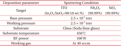
Deposition conditions of Nb2O5, SiO2, and ITO films by RF magnetron sputtering.
In order to select the Nb2O5 and SiO2 buffer layer thicknesses, the Essential Macleod Program (EMP) was adopted. The simulation was designed with variable parameters such as wavelength (400~700 nm) and thickness of layers [Nb2O5 (5~30 nm)|SiO2 (40~65 nm)|ITO (40 nm)]. The surface morphology of the films was investigated by Atomic Force Microscope (AFM) measurements in contact mode. The transmittance and reflectance of the films were measured using a UV-VIS-NIR spectrophotometer (KONICA-MINOLTA CM-3600d) in the 400~700 nm wavelength range. The sheet resistance and the resistivity of the samples were calculated using the four-point probe method (KEITHLEY 2700 multimeter/data acquisition system). In addition, the interfacial properties of the optimized [Nb2O5 (20 nm)|SiO2 (45 nm)|ITO (40 nm)] electrodes were analyzed using (AES) depth profiling.
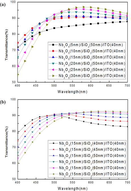
An Essential Macleod Program (EMP) was adopted to optimize the Nb2O5 and SiO2 buffer layer thicknesses. Figure 1 shows the transmittance of [Nb2O5 (5, 10, 15, 20, 25, 30 nm)|SiO2 (40, 45, 50, 55, 60, 65 nm)|ITO (40 nm)] multi-layer films from 400 to 700 nm wavelength using the EMP method. Based on EMP simulation, the [Nb2O5 (10, 15, 20 nm)|SiO2 (45, 50, 55 nm)|ITO (40 nm)] multi-layered thin film exhibited a high average transmittance of more than 85% in the visible region (400~700 nm).
Figure 2 presents the typical simulated optical transmittance of the [Nb2O5 (15 nm)|SiO2 (50 nm)|ITO (40 nm)] film using the EMP program and the measured optical transmittance of the [Nb2O5 (15 nm)|SiO2 (50 nm)|ITO (40 nm)] multi-layer film, respectively for comparison. The transmission spectra were measured with a UV-VIS-NIR spectrophotometer in the 400~700 nm wavelength range. Compared with the EMP simulation result, the experimental results matched relatively well with the simulated results, showing a similar tendency in terms of different wavelengths. The simulated and measured transmittances of the [Nb2O5 (15 nm)|SiO2 (50 nm)|ITO (40 nm)] film were in the range of about 87% ~ 92% at 550 nm wavelength.
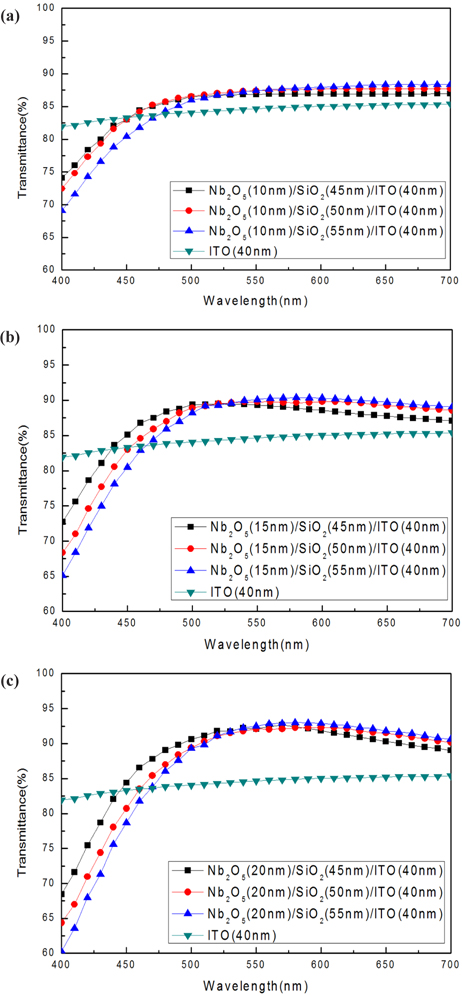
Figure 3 shows the transmittance of the ITO films with different [Nb2O5|SiO2] buffer layers in the wavelength range of 400-700 nm, with the ITO single layer as the reference. The glass substrate has a 95% transmittance at 550 nm, whereas the ITO films with Nb2O5 and SiO2 buffer layers deposited on glass have a transmittance of about 85%~88% at 550 nm. As seen in Fig. 3, the film transmittance decreased slightly in the 400~500 wavelength range when the Nb2O5 and SiO2 buffer layer thicknesses increased, possibly due to the increase in absorption of the buffer layers. As a result of using the buffer layer, the transmittance of the multi-layer films was 5% higher than that of the ITO single layer.
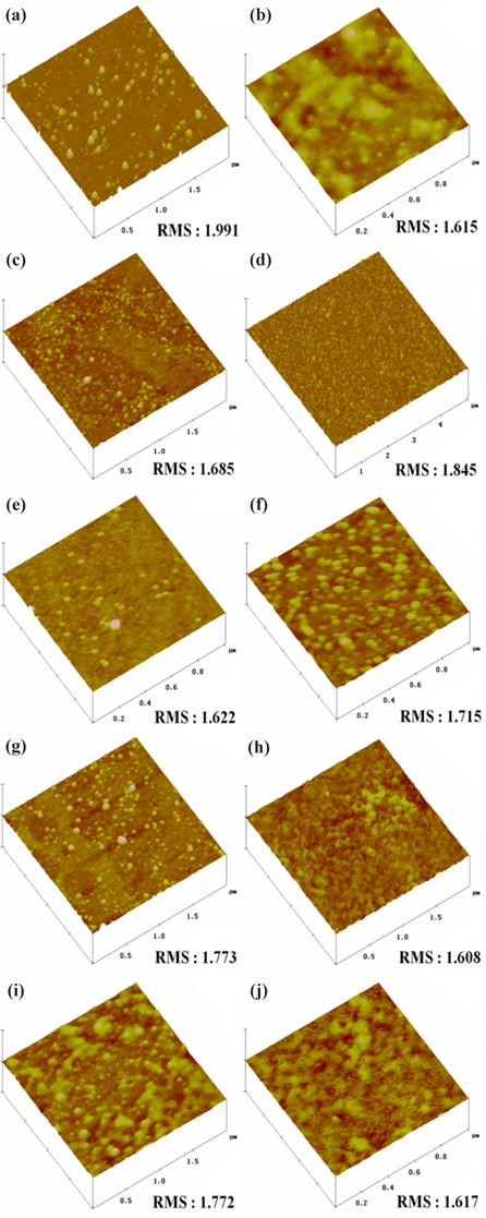
The morphology of the deposited films was investigated using AFM. Fig. 4 shows AFM images of the ITO single layer and [Nb2O5|SiO2|ITO] multi-layer films. The thickness of the ITO films was kept at about 40 nm. It can be seen that the surface roughness of the ITO films was related to that of the underlying buffer layer. A relatively large RMS value appeared for the ITO film deposited directly on the glass substrate. The pre-deposition of the Nb2O5 and SiO2 buffer layer decreased the surface roughness of the glass substrate, resulting in a decrease of the RMS value of the ITO films. Atoms grow preferably in sunken regions on the substrate. Surface roughness maintained a relatively small value in the range of 0.1~0.4 nm, using Nb2O5 and SiO2 buffer layers. The net effect is that the ITO film with the Nb2O5 and SiO2 buffer layers has the smoothest surface.
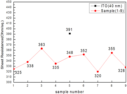
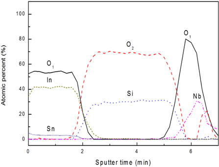
Figure 5 shows the effect of Nb2O5 and SiO2 buffer layer thicknesses on the sheet resistivity of the ITO films. Table 2 presents the sample numbers in terms of Nb2O5 and SiO2 film thicknesses. The ITO single layer has a 391 Ω/sq. sheet resistance, and the ITO films with Nb2O5 and SiO2 buffer layers deposited on glass show a sheet resistivity of about 330~343 Ω/sq. A comparison of the RMS in Fig. 4(h) shows that ITO films with Nb2O5 (20 nm) and SiO2 (45 nm) buffer layers have the smoothest surface. We assume the decrease of sheet resistance in the ITO film with an optimized buffer layer is related to the change of ITO surface morphology. It was known that a smoother surface has a positive effect on decreasing resistivity [23]. Fig. 6 shows the AES depth profiles of the optimized [Nb2O5 (20 nm)|SiO2 (45 nm)|ITO (40 nm)] electrodes on the glass substrate. Based on AES data, each Nb2O5 and SiO2 ITO region is relatively well defined and no typical and distinguishable interfacial diffusion is observed between each layer.
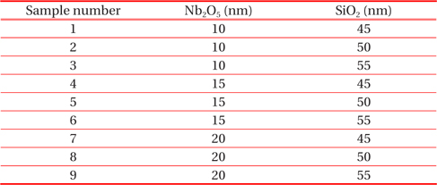
[Table 2.] Sample number in terms of Nb2O5 and SiO2 film thickness.

Sample number in terms of Nb2O5 and SiO2 film thickness.
The effects of the thickness of the Nb2O5 and SiO2 buf fer layer on the optical, structural, and electrical properties of ITO films on glass substrates were investigated. An improvement in the electrical resistivity of ITO film was achieved by applying a [Nb2O5|SiO2] buffer layer between the ITO film and the glass substrate. The resistivity of the films decreased from 391 Ω /sq. to 320 Ω /sq. when the [Nb2O5|SiO2] buffer layer produced at a deposition thickness of 20 nm and 45 nm was applied. ITO films with 20 nm thick Nb2O5 and 45 nm thick SiO2 buffer layers have the lowest sheet resistance (320 Ohm/sq.). During the degree of crystallization, the decrease in surface roughness was beneficial to the enhancement of electrical properties. The [Nb2O5|SiO2] buffer layers have little effect on the optical transmittance of all the ITO films. Compared with the transmittance of an ITO single layer film, the transmittance of [Nb2O5|SiO2|ITO] multi-layer films increased slightly in the visible range of 400~700 nm. We can conclude that the structural, optical, and electrical studies reveal that [Nb2O5|SiO2] buffer layers play a key role in increasing the transmittance of ITO thin films.

![Simulated optical transmittance spectra of ITO films with Nb2O5 and SiO2 buffer layers of different thicknesses; (a) [Nb2O5(5-30 nm)|SiO2(50 nm)|ITO(40 nm)] and (b) [Nb2O5(15 nm)|SiO2(40-65 nm)|ITO(40 nm)].](http://oak.go.kr/repository/journal/15561/E1TEAO_2015_v16n1_29_f001.jpg)
![Simulated optical transmittance of the [Nb2O5(15 nm)|SiO2(50 nm)|ITO(40 nm)] film using the EMP program and the measured optical transmittance of the [Nb2O5(15 nm)|SiO2 (50 nm)|ITO(40 nm)] multi-layer film for comparison.](http://oak.go.kr/repository/journal/15561/E1TEAO_2015_v16n1_29_f002.jpg)
![Dependence of the sheet resistance for ITO films on the [Nb2O5|SiO2] buffer layer thickness ; (a) ITO single layer; (b) Nb2O5(10 nm) | SiO2(45 nm); (c) Nb2O5(10 nm) | SiO2( 50 nm); (d) Nb2O5(10 nm) | SiO2(55 nm); (e) Nb2O5(15 nm) | SiO2(45 nm); (f) Nb2O5(15 nm) | SiO2(50 nm); (g) Nb2O5(15 nm) | SiO2(50 nm); (h) Nb2O5(20 nm) | SiO2(45 nm); (i) Nb2O5(20 nm) | SiO2(50 nm); (j) Nb2O5(20 nm) | SiO2(55 nm).](http://oak.go.kr/repository/journal/15561/E1TEAO_2015_v16n1_29_f005.jpg)
![AES depth profiles of [Nb2O5|SiO2|ITO] multi-layer film grown on a glass substrate under an optimized condition.](http://oak.go.kr/repository/journal/15561/E1TEAO_2015_v16n1_29_f006.jpg)