Amorphous oxide semiconductor (AOS) such as ZnO-based thin film transistors (TFTs) have attracted much attention for their application to integrated circuits used in backplane of active matrix displays. They have higher electrical and optical property than that of amorphous silicon thin film transistors (a-Si TFTs), and their production cost is low compared with the low-temperature polycrystalline silicon (LTPS). Recently, there have been many reports on different materials for active layer of AOS TFTs. Among them, the most extensively used material is amorphous indium-gallium-zinc-oxide (a-IGZO). The a-IGZO TFTs exhibit high field effect mobility (>10 cm2 /V s) in the mobility enhancer like indium [1]. However, indium is an expensive and rare material. Therefore, indium-free materials like zinc tin oxide (ZTO), have been studied intensively in these days [2,3]. Most of AOS TFTs are annealed for the improvement of electrical performance and stability of device, after deposition at room temperature (RT). Therefore, it is very important to optimize the annealing process [4,5].
Through our studies and reference of other groups, we expected that hydrogen is not only used for generation of free electrons but also for the passivation effect of oxygen vacancy. However, the role of hydrogen in the wet annealing treatment is not clear yet, so the study is still in progress.
In this paper, we have fabricated silicon zinc tin oxide (SZTO) TFTs without indium, and we have annealed and compared them in the air and in wet ambient. TFTs have been annealed followed by the completed fabrication of SZTO TFT, and the performance of TFT has been compared by the annealing conditions.
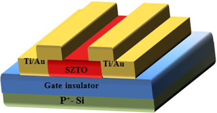
SZTO films were deposited by radio frequency (RF) magnetron sputtering on a SiO2(200 nm)/p-type Si(heavily doped) substrate at room temperature with the bottom gate structure. Figure 1 shows the schematic diagram of SZTO TFT structure. The magnetron sputtering was conducted in a mixed atmosphere of O2 and Ar (flow rate ratio of 1:9), by supplying an RF power of 50 W. The SZTO film thickness was about 40 nm and was patterned by using photolithography. The width and length of the channel are 250 μm and 50 μm, respectively. After deposition of the SZTO films, source and drain electrodes (Ti/Au=10 nm/50 nm) were fabricated by e-beam evaporation and lift off process. Then, annealing process was performed in different annealing conditions, such as in air and in wet ambient.
The SZTO TFT was annealed at 500℃ for 2 h. Air annealing treatment was performed in atmospheric condition, while wet annealing was performed in the ambient of heated de-ionized (DI) water.
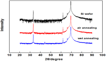
The amorphous structure of SZTO thin films was confirmed by X-ray diffraction (XRD). All electrical performances and stress characteristics were measured by using a semiconductor parameter analyzer (EL-423).
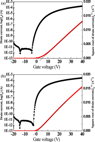
Figure 2 shows XRD patterns of SZTO thin films on heavily doped p-type Si wafer. Most of the peaks are well-agreed with those of Si wafer peaks. We confirmed amorphous structure of SZTO thin films [6,7]. Transfer characteristics of air and wet annealed SZTO TFTs measured at VDS=5.1 V are shown in Fig.3. Gate voltage (VGS) was swept from –20 V to 40 V. Transfer curve shows drain current of log plot (black line) and linear plot (red line). We deduced threshold voltage (Vth) by extrapolation method in the linear plot. Table 1 shows the electrical performance of SZTO TFTs with different annealing condition. The field-effect mobility (μFE) was calculated by using the following relation: [8]
[Table 1.] Electrical performances of SZTO TFTs with different annealing conditions.
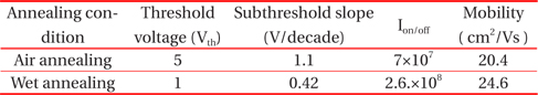
Electrical performances of SZTO TFTs with different annealing conditions.
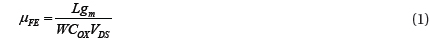
Where, VDS is drain voltage, gm is the transconductance, Cox is the oxide capacitance of the gate insulator, W and L are channel width and length, respectively.
In the case of air annealing, the threshold voltage (Vth), subthreshold slop (SS), drain current on/off ratio (Ion/off), and μFE were measured to be about 5 V, 1.1 V/decade, 7 × 10⁷ , and 20.4 cm2 /V s, respectively. For the wet annealing, the Vth, SS, Ion/off, and the field effect mobility were measured to be about 1 V, 0.42 V/ decade, 2.6. × 108 and 24.6 cm2 /V s, respectively. Based on these results, it is interesting to note that wet annealing treatment can improve the electrical characteristics of the device. This is understood from the generation of free electrons by adopting wet annealing process. Two possible mechanisms could be proposed to explain the performance improvement.
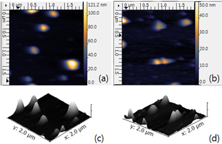
One of the mechanisms is oxygen atoms of a-SZTO film reacting with neighboring hydrogen to generate H2O. This mechanism can be described as follows: [9]

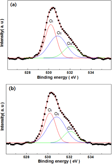
where, Vo ·· is an ionized oxygen vacancy, and e- denotes free electron. The second possibility is the carrier injection by the adsorption of H2O on the a-SZTO surface. H2O adsorption donates a partial negate charge to the channel surface with either molecules or hydroxyl forms [10]. In this case, the role of H2O could be defined as a donor. Consequently, carrier concentration is increased by wet annealing process. Sub-threshold slope value of wet annealed SZTO TFTs is smaller than that of air annealing treatment. This result can be understood more in detail by analyzing the surface roughness. Figure 4 shows AFM images of air and wet annealed SZTO thin films. The root-mean-squares (RMS) surface roughnesses are measured to be about 16.1 nm and 5.23 nm with air and wet annealing, respectively. It shows that surface roughness has been improved more by wet annealing than by air annealing treatment [11]. Figure 5 shows the comparison between the O1s peaks of XPS for the air and wet annealed SZTO thin films. We de-convoluted the O1s peaks into three Lorentzian-Gaussian peaks. The peaks centered at the binding energies of 530 eV (OI), and 531 eV (OII), and 532 eV (OIII) were attributed to oxygen ion bonded with neighboring metal atoms, and oxygen vacancy, and presence of loosely bound oxygen on the surfaces such as H2O and OH groups, respectively. The OII peak value for the air and wet annealed devices were 41.4% and 48.5%, respectively, as summarized in Table 2. The area of the oxygen vacancy related peak increased with wet annealing, compare with air annealing. This result is well agreed with the mechanisms described above.
In summary, we have fabricated the amorphous SZTO TFTs by RF magnetron sputtering process, and annealed in the air and the wet ambient. The Vth, SS, and μFE were improved by about 4 V negative shift, 0.68 V/decade, and 4.2 cm2 /V s, respectively, after wet annealing treatment compared with air annealing treatment. In addition, XRD and XPS data showed the amorphous structure of SZTO thin films and the increase of oxygen vacancy. Through this result, it is expected that wet annealing process can improve on the device performance by increasing the free electron concentration.