In radar systems demanding high resolution, a single-pole double-throw (SPDT) RF switch is indispensable because radar systems generally use a single antenna to transmit and receive signals for a transceiver module. The SPDT RF switch determines the performance of the radar and demands a high isolation level and low insertion loss.
It is very difficult to suppress the signal leakage that is generated when the RF switch is turned on. Therefore, the RF switch requires high isolation and low insertion loss differently from the general switches used in digital systems or high power systems. Signal leakage is a critical cause for the degrading isolation and insertion loss [1]. Generally, a switch is produced using metal oxide semiconductor field effect transistors (MOSFET) because the insertion loss can be at a very low level (around 0 dB). However, at high frequencies (over 1 GHz), as the insertion loss is degraded, isolation also decreases, leading to difficulties in designing SPDT. Therefore, in this paper, a highisolation RF SPDT switch that maintains a low insertion loss is presented. A leakage signal cancellation method with inductive switching is proposed for obtaining high isolation using an 0.18-μm SiGe HBT process.
II. THE PROPOSED SPDT RF SWITCH
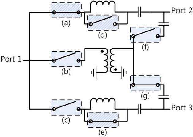
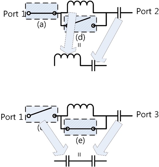
Fig. 1 shows the configuration of the proposed SPDT RF switch, where the switches from (a) to (e) were designed using MOSFETs and the switches from (f) and (g) were designed using HBT. The RF signal is transmitted from port 1 to port 2 or vice versa, while port 3 is isolated. Meanwhile, the signal is transmitted from port 1 to port 3 instead, and the switches from (a) to (g) operate in opposite to the aforementioned condition.
The switches of (a) and (c) are prepared to control the path of the signal from port 1 to port 2 or port 3. When the signal is transferred from port 1 to port 2, (a) should be closed and (c) should be open. Because switch (b) is used for trapping signal leakage, it should stay off. The leakage signal entering from switch (b) goes through the inverter located between switches (b) and (g). The inverter is connected to switches (f ) and (g), which are used to cancel the signal from the isolated port.
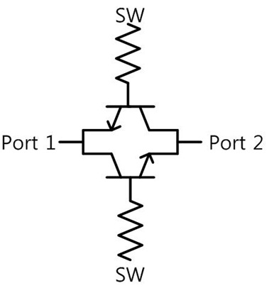
Fig. 2 illustrates the MOSFET switch used for (a) to (e) as shown in Fig. 1, which can be composed of general switches [2,3]. They are turned on and off by toggling the voltage of the SW in Fig. 2.
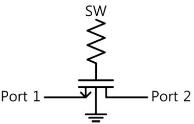
Fig. 3 shows the HBT switch used for (f) and (g) in Fig. 1. Since in bipolar junction transistors, the current flows from the collector to the emitter, the switch composed of HBT can use the configuration as devised in Fig. 3 to flow current in both directions. Because the switch using HBT has a high insertion loss, it is not widely used. However, since it shows high isolation, the HBT switch can be used only for obtaining a high isolation level [4,5], whereas the MOSFET switch can be utilized for low loss application as described in Fig. 1.
When designing the RF switches, it is difficult to increase the isolation while sustaining low insertion loss because of the parasitic capacitances among the gate, drain, and source. As the frequency and width of the MOSFETs increase, isolation becomes aggravated. However, if the width of the MOSFETs shrinks to increase isolation, insertion loss increases. Therefore, the proposed RF switch uses a leakage cancellation method to increase isolation.
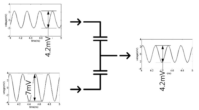
For example, when port 1 and port 2 are connected together through switches, (b) and (c) in Fig. 1 are open. However, some amount of the signal sneaks into port 3, which is called leakage, because of the capacitance between the drain and the source. Signal leaking through switch (b) enters the inverter and passes through switch (g), finally coming out of port 3. This signal is eventually cancelled with the leaking through switch (c) and passing through switch (e) since both signals leaking through (b) and (c) are 180° out of phase. The cancellation of the two signals transferred by the capacitor at port 3 is demonstrated in Fig. 4 in more detail.
In addition to leakage signal cancellation, the inductive switching method is used for switches (d) and (e). For the switches in Fig. 1 to work properly, port 1 and port 2 must be matched to 50 Ω using series inductors and capacitors. Otherwise, by closing switch (e), impedance matching would no longer be maintained. In addition, as explained in Fig. 5, the path from port 1 to port 2 becomes composed of the
While leakage signals through (b) and (c) are cancelled at port 3, the insertion loss from port 1 to port 2 increases because of switch (f), the parasitic capacitances, and the inverter. Through this mechanism, the signal through switch (a) is a little degraded. Because the HBT switch shows high isolation characteristic, the signal passing from port 1 to port 2 is not very affected by switch (f) and the leakage signal from port 1 to port 3 can be effectively suppressed. Therefore, the insertion loss is maintained up to approximately 1 dB.
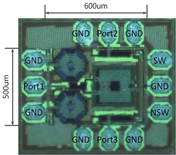
III. SIMULATION AND MEASUREMENT RESULTS
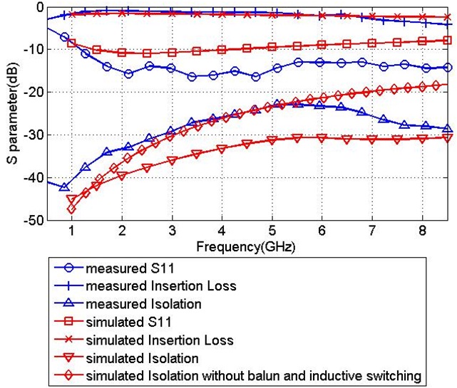
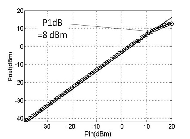
As shown in Fig. 6, the insertion loss obtained is 2 dB or less over the entire frequency range of 1 to 8 GHz for both the simulation and measurement. On the other hand, the measured isolation level is considerably high (approximately 23 to 40 dB) in the frequency range of interest after the leakage signal cancellation and inductive switching are applied. By using inductive switching and leakage signal cancelling, isolation is enhanced by 2 to 11 dB in the frequency range of interest in the simulation. In addition,
[Table 1.] Performance summary and comparison with previous work
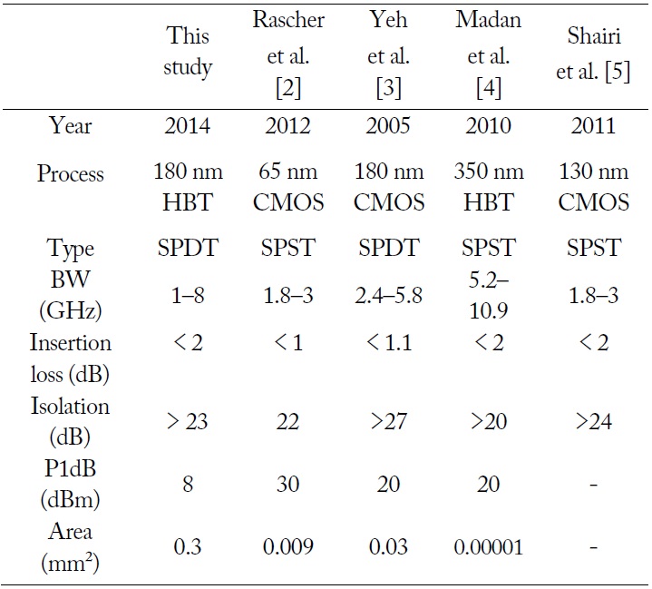
Performance summary and comparison with previous work
In conventional RF switches using MOSFETs, insertion loss increases as isolation increases. However, the proposed RF switch employs a leakage cancellation method to improve isolation and decrease insertion loss, thereby maintaining a wideband working range. Insertion loss is maintained at less than 2 dB in the 1 to 8 GHz range, while the isolation obtained is considerably high.