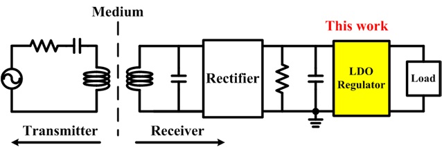
The design of power management in system-on-chip (SoC) for a wireless power transfer (WPT) system is now in active progress. The high-performance voltage regulation in terms of accuracy, power efficiency, response time, silicon area, and the off-chip component free feature is vital for power management in SoC. Of all types of voltage regulators, the low-dropout (LDO) regulator is regarded as a suitable choice for on-chip voltage regulation due to its fast transient response, low noise, and high stability and could be used as a building block for a WPT system receiver as shown in Fig. 1.
Because conventional LDO regulators for the receiver of a WPT system have been constituted with feedback topology (made up of voltage reference, error amplifier, and power device), frequency compensation is additionally required for closed-loop stability. This closed-loop stability is usually achieved with an off-chip capacitor’s equivalent series resistance (ESR), which provides zero ESR for its open-loop transfer function and contributes pole-zero cancellation [1]. However, the stability significantly depends on the ESR, which cannot be easily controlled and changes with temperature. The off-chip capacitor is the main obstacle for the full integration of LDO regulators in SoC design. To resolve this issue, capacitor-free LDO regulators have been reported in [2-7].
In LDO regulator design, accuracy and low-voltage dropout can be complemented by using the pass transistor, which is designed with a large transistor. The stability and phase margin can be improved by adding a Miller capacitor at the output stage of the error amplifier. However, parasitic capacitance around the large pass transistor and the Miller capacitor added for improving stability is seen as the output capacitance of the error amplifier and generates slewing, which slows the response of the pass transistor. This Miller capacitor provides a trade-off between stability and fast response. Since the receiver of a WPT system should produce electric power that responds quickly to inconsistent input power, a fast response is more important than stability. Therefore, the Miller capacitor was not employed for obtaining a fast response in this work. Based on this design philosophy, we designed an error amplifier with dynamic current biasing to improve the slew rate and verified the fast response and accuracy of the LDO regulator by using the proposed error amplifier with abrupt input changes.
II. CIRCUIT DESIGN AND ANALYSIS
1. Conventional LDO Regulators
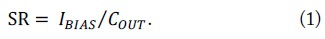
Fig. 2 shows the block diagram of conventional LDO regulators. The most important feature of LDO regulators is the dropout voltage. To address this, the aspect ratio of the pass transistor is designed very large. As the parasitic capacitances (
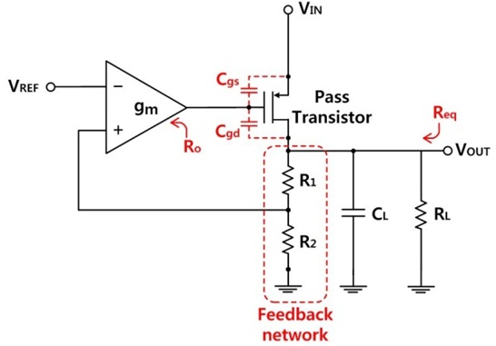
The operational amplifier used for the error amplifier in Fig. 2 demonstrates a large output capacitance that causes slewing, as illustrated in Fig. 3. When the step input voltage is applied to

The error amplifier plays a crucial role in controlling the gate voltage of the pass transistor by rapidly detecting the change in output voltage against the reference voltage. A controlled gate voltage regulates the channel of the pass transistor, changing the current and dropout voltage. Therefore, slewing of the error amplifier prevents the quick detection of rapid change at the input. A method is needed to reduce the slew rate in order to improve accuracy and response of the LDO regulator. Based on Eq. (1), the slew rate can be enhanced by increasing the bias current.
As known from Eq. (1), the error amplifier of an LDO regulator requires more bias current to resolve slewing, and this can increase power consumption due to the excessive current. Thus, dynamic current biasing is proposed to improve the slew rate of an LDO regulator without consuming additional current.
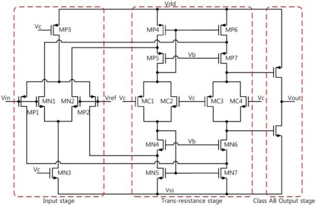
Fig. 4 shows the CMOS rail-to-rail cascode amplifier working as an error amplifier of the LDO regulator. The first stage (input stage) designed in the rail-to-rail structure converts the input voltage to current. The second stage (trans-resistance amplifier stage), composed of a class-AB amplifier operating over a wide range, amplifies the converted current from the first stage, eventually controlling the pass transistor. The output of the LDO regulator is fed back to the input of the error amplifier since abrupt voltage change at the input needs to be detected in time [8].
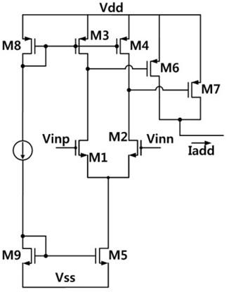
The proposed dynamic current biasing is described in Fig. 5, which shows that current does not flow in a steady state but increases when slewing arises. The dynamic current bias circuit is composed of differential inputs (M1–M5) that can sense slewing and sub-current sources (M6, M7) that cause additional bias current. Operation of this dynamic current bias circuit is as follows:
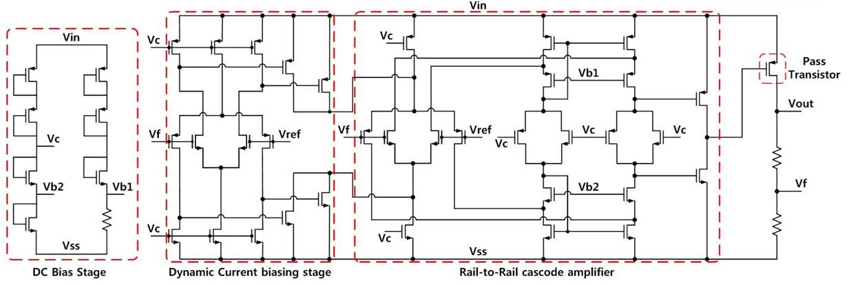
Fig. 6 shows the final LDO regulator combined with the proposed CMOS rail-to-rail cascode amplifier as shown in Fig. 4 and the dynamic current bias circuit as proposed in Fig. 5.
III. SIMULATION AND MEASUREMENT RESULTS
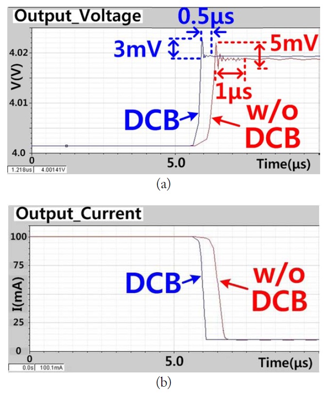
Load transients for an LDO regulator employing dynamic current biasing werefirst simulated to comparewith load transients without dynamic current biasing. Fig. 7 demonstrates the simulated results. The load transient improved from 5 mV to 3 mV, and the settling time also improved from 1 μs to 0.5 μs. Results showed that the overall response from load variation was faster when dynamic current biasing was applied to the LDO regulator.
Line transients using 4.3–6 V input were also simulated for LDO regulators with and without dynamic current biasing. As shown in Fig. 8, the line transient improved from 100 mV to 90 mV, and settling time increased from 2 μs to 0.5 μs as expected.
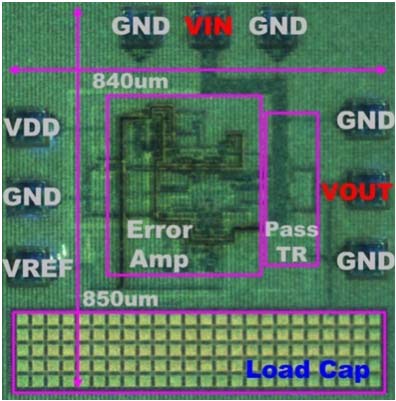
The proposed LDO regulator was fabricated with Dongbu 0.35 μm BCDMOS technology. Fig. 9 shows a microphotograph of the proposed LDO regulator with an area of 840 μm × 850 μm. This LDO was mounted on a 100-pF capacitor loaded inside the chip.
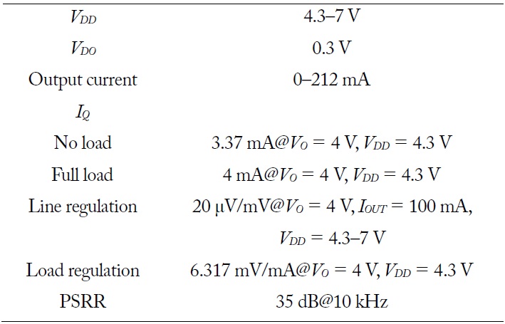
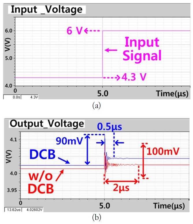
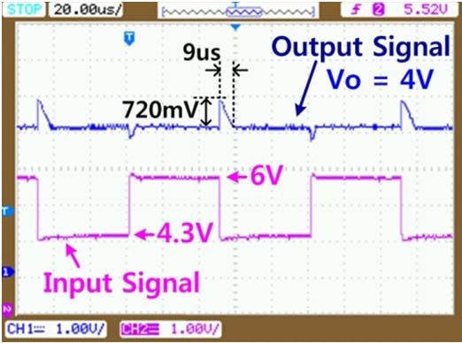
The measured result of theline transient with a 100-pF output capacitor is shownin Fig. 10 and the perfornamce summary is providedin Table 1. The design concept of this proposed LDO regulator is for low-power consumption, but the measured current consumption was 4 mA, which is much larger than expected. Whereas an unnecessary large amount of current is consumed in the bias stage (shown in Fig. 6), which is contrary to the design goal, the error amplifier does not consume much current (less than 100 μA in simulation).
[Table 1.] Performance summary

Performance summary
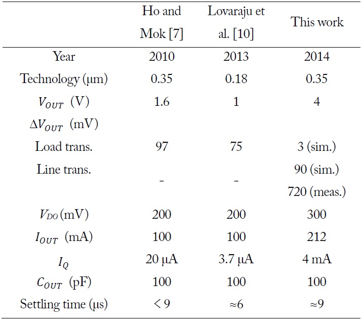
When the output voltage was 4 V, the input voltage had a wide range of about 4.3–7 V and the dropout voltage was about 300 mV. Power supply rejection ratio was obtained as 35 dB at 10 kHz. The overshoot of the LDO regulator was measured in terms of line transient at about 720 mV becausea large input voltge was used, as demonstrated in Fig. 10. Although a highto- low transition was used for measurement, which is opposite to the simulation, the measured results were the same as those of the simulation. Settling time was obtained as 9 μs for an input voltage of 4.3–6 V, as illustrated in Fig. 10. This is a much faster settling time for a 1.7-V input variation compared to work by other researchers. More results are compared in Table 2. Except for current consumption, all other performances are comparable to others’ previously pubished circuits.
[Table 2.] Comparison of low-dropout (LDO) regulators

Comparison of low-dropout (LDO) regulators
We proposed an LDO regulator with dynamic current biasing in order to enhance the slew rate. The dynamic current biasing is notturned on in the absence of slewing but acts to enhance the slew rate when slewing occurs. In addition, the input stage of the error amplifier with rail-to-rail structure has a wide range of 4.3–7 V. The linetransient can be recovered within 9 μs foran input voltage with a range of 4.3–6 V.