검색 전체 메뉴
PDF
맨 위로
OA 학술지
Ultra Broadband Absorption of SPPs Enhanced Dual Grating Thin Film CIGS Solar Cell Enabled by Particle Swarm Optimization
  • 비영리 CC BY-NC
  • 비영리 CC BY-NC
ABSTRACT
Ultra Broadband Absorption of SPPs Enhanced Dual Grating Thin Film CIGS Solar Cell Enabled by Particle Swarm Optimization
KEYWORD
Solar cell , CIGS , Grating , SPPs
  • I. INTRODUCTION

    Among various thin film solar cells progressing more rapidly, the polycrystalline chalcopyrite CuIn1-xGaxSe2 (CIGS) is a one of the most attractive candidates due to low material cost, long-term thermal stability, large-scale and flexible manufacturing, and superior conversion efficiency [1-4]. In particular, compared to other thin film solar cells based on a-Si or polymers, the highest conversion efficiency of up to 20.3% [5] is a result of the unique material properties of CIGS as the I-III-VI2 semi-conducting compounds, in which the bandgap energy range can be controlled by ratio x≡Ga/(In+Ga) [4, 6-7].

    Recently, one of most attractive methods for enhancing light trapping in thin film solar cells is to utilize the effect of surface plasmon polaritons (SPPs) by applying metallic nanostructures [8-12]. The excited SPPs cause strong nearfield enhancement and increase optical path length via broad-angle light scattering. Because the dissipation energy is proportional to the electric field intensity, the strongly confined energy at the interface between metallic element and active medium boost solar cell efficiency. For example, metallic nanogratings placed at the bottom of the active layer [11-12] enable the broadband and polarization insensitive absorption by taking advantage of effective coupling to SPP (plasmonic) or photonic modes. Meanwhile, metallic nanogratings or nanoparticles placed at the top surface of the active layer also increase absorption performance although the effect can occur only at certain wavelengths and a considerable amount of incident light is blocked by metallic elements. To further improve absorption performance compared to these single nanogratings based structures, recently, there has been growing interest in using dual grating structures to enhance absorption thin film solar cells [13-16]. These structures will enhance the coupling between incoming light and different types of resonance modes, by changing geometry parameters of dual grating structures (top and bottom), resulting in an overall broadband absorption enhancement.

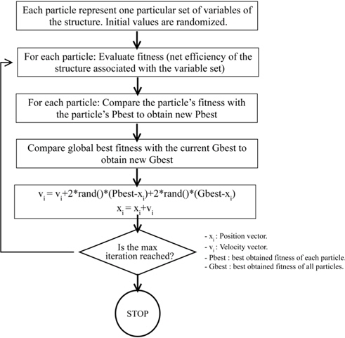
    Most previous works on optimization of grating structures used a parametric scan method to enhance absorption [10, 12-13]. It becomes a much more difficult and time-consuming process when the number of relevant geometric parameters increases. In this study, we demonstrate the maximal utilization of the ‘particle swarm optimization (PSO)’ method for a thin film CIGS solar cell with the dual nanogratings composed of a top CIGS grating and a bottom Ag grating, which have 7 degrees of freedom (active layer thickness, period, each thickness and width of top and bottom gratings, and the lateral shift between both gratings). The PSO method, developed by Kennedy and Eberthart [17], was a robust stochastic optimization technique. Inspired by social behavior of bird flocks or fish schools, PSO has been used for various design optimization problems, including diffractive grating structures [18-20]. PSO is particularly well suited to the optimization of solar cell designs due to the fact that PSO is a metaheuristic algorithm - no assumption is necessary on the topology of the search space - which can be quite complicated when complex structures are employed to maximize performance. The flowchart of the PSO algorithm employed in this paper is shown in Fig. 1.

    Due to well-spaced and well-defined absorption peaks obtained from PSO, the optimized shifted dual grating structure exhibits the broadband absorption at the wide range wavelengths from 300 nm to 1200 nm, with the net absorption of A = 85.6% and A = 78.1% for TM only and for both TM and TE polarizations, respectively. In this paper, well-spaced absorption peaks mean the peaks’s wavelengths are positioned in such a way that the entire absorption spectrum is divided into equally (or roughly equally) spaced regions. Well-defined absorption peaks means the absorption peaks achieve maximum total absorption of 100%.

    II. DEVICE ARCHITECTURE AND NUMERICAL METHOD

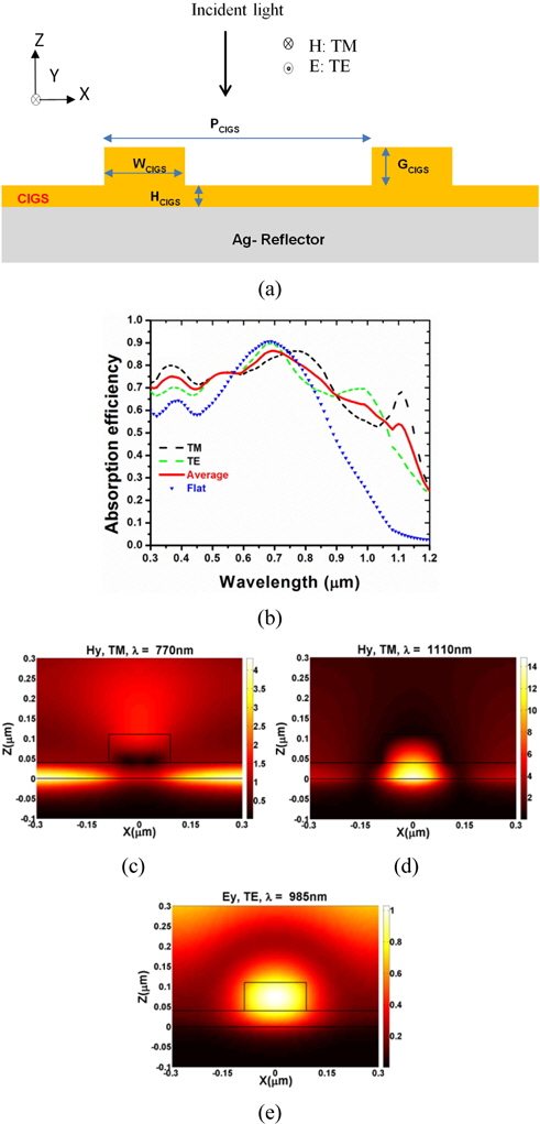
    A thin film solar cell device using shifted dual grating structure was designed with the silver grating in the bottom and the CISG grating on the top. The WAg and GAg are the width and thickness of the silver grating. The WCIGS and GCIGS are the width and thickness of the CIGS grating. In all calculations, the silver reflector thickness is 100 nm and the incident light is normal to the surface. The optical constants of CuIn1-xGaxSe2 (x = 0.31) and silver are extracted from Ref. [7] and [21], respectively. The absorption efficiency (a(λ )) as a function of wavelength in an active layer is investigated using rigorous coupled wave analysis (RCWA) based commercial software, DiffractMOD. To evaluate solar cell performance, the net absorption efficiency (A) is also calculated by taking into account the standard AM 1.5G solar illumination (S(λ )), as follows:

    image

    III. OPTIMIZATION OF SINGLE GRATING STRUCTURES

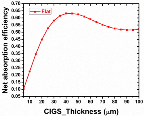
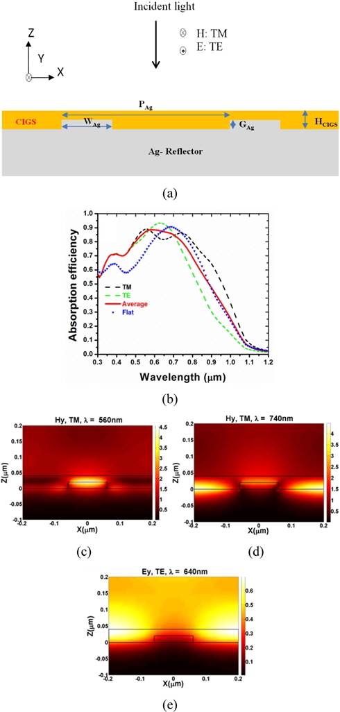
    In this section, we examine absorption performances of two single (top and bottom) grating based structures by using ‘parametric scan’ as the optimization method under both polarizations. We fixed the CIGS layer thickness to HCIGS = 40 nm, at which net absorption has a highest value of A = 63.2% in flat structure (Fig. 2). Due to the effect of a Fabry-Perot-like resonance caused by the reflector and the surface of a flat solar cell, increasing the thickness of the CIGS layer does not always increase its performance.

       3.1. Bottom Grating

    The schematic of bottom grating structure is shown in Fig. 3(a). For the purpose of maximizing the net absorption efficiency, we employed the parametric scan for period range of PAg from 100 to 900 nm with 100 nm intervals, fill factor range of FAg from 0.1 to 0.7 with 0.1 intervals, and grating thickness range of GAg from 5 to 35 nm with 5 nm intervals. This means that calculations of 9×7×7 times are conducted. The optimized averaged A of 66.8% is obtained in the case of PAg = 400 nm, FAg = 0.3 (WAg = 120 nm), GAg = 20 nm. Figure 3(b) shows the absorption efficiency spectra of optimized bottom grating structureand optimized flat structure with HCIGS = 40 nm for both polarizations. There are two absorption peaks for TM wave at wavelength range of 500 to 800 nm. The magnetic field profiles (Fig. 3(c) and 3(d)) reveal that the absorption peaks at λ= 560 nm and λ= 740 nm correspond to SPPs modes characterized by strongly confined fields at interface between silver and CIGS layer. For TE polarization, absorption peak at λ= 640 nm originates from waveguide mode coupling, as estimated from strong electric field confined in only the CIGS layer in Fig. 3(e).

       3.2. Top Grating

    The optimization process using the parametric scan was also conducted for the top grating, while keeping the similar parametric ranges to the bottom grating; period range of PCIGS from 100 to 900 nm with 100 nm intervals, fill factor range of FCIGS from 0.1 to 0.7 with 0.1 intervals, and grating thickness range of GAg from 10 to 70 nm with 5 nm intervals. The schematic of top grating structure is shown in Fig. 4(a). At PCIGS = 600 nm, FCIGS = 0.3 (WCIGS = 180 nm), and GCIGS = 70 nm, the optimized averaged A of 73.35% is obtained. Fig. 4(b) shows the absorption efficiency spectra of optimized bottom grating structure and optimized flat structure with HCIGS = 40 nm for both polarizations. The optimized top grating presents two SPPs absorption peaks in the longer wavelength range under TM polarization, as shown in Fig. 4(b). The absorption peaks at λ= 770 nm and λ= 1110 nm come from SPP mode coupling, as estimated from strong field confinement at the interface between silver and CIGS layer in Fig. 4(c) and 3(d) respectively, similar to bottom grating case. For TE polarization, coupling of waveguide mode into CICS grating element occurs at λ= 985 nm (seen in Fig. 4(e)).

    IV. DUAL GRATING STRUCTURES

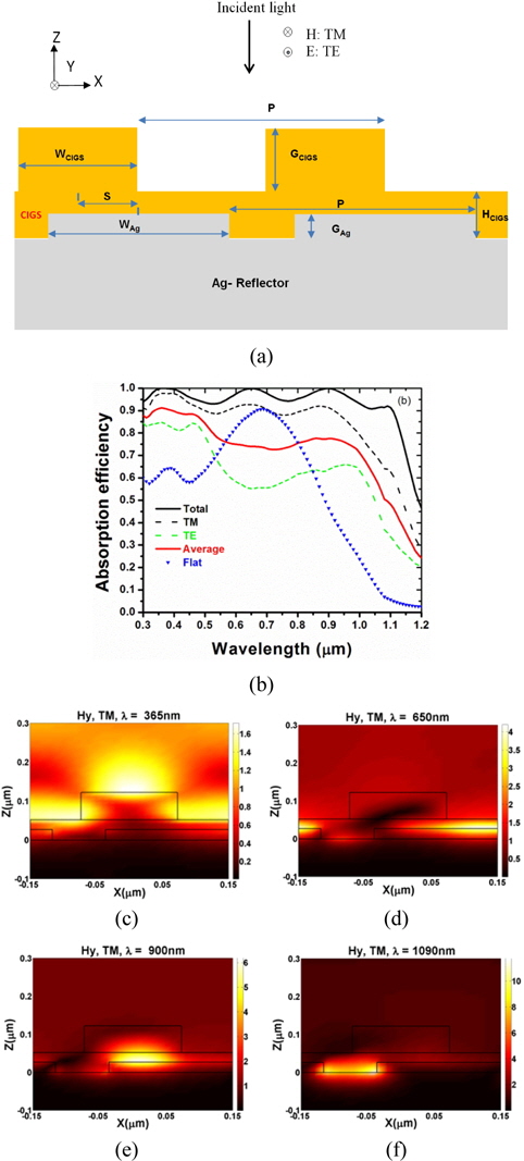
    Now, we address the dual grating structures. Under the limitation of the design tools, we restricted the period of the top and bottom gratings to be the same. The double grating structure has 7 degrees of freedom; active layer thickness (HCIGS), period (P), each thickness (GCIGS, GAg) and width (WCIGS , WAg) of gratings, and the lateral shift (S) between both gratings. To reliably, albeit roughly, estimate the global optimization, the parametric scan can be attempted, similar to the single grating case of previous section. Assuming that each parameter has 10 steps, total number of iterations would be 107 (10 million); it is a prohibitive value which is highly time-consuming.

    Also, separated tuning of each parameter, as done in [13], is not the answer; changing one design parameter would almost certainly shifts the local optimal value of all of the remaining parameters, rendering the search for the global optimum value impossible. Indeed, in [22], virtually any absorption in the active layer was not obtained from 700 nm to near infrared, where strong plasmonic modes can be potentially excited.

       4.1. PSO Optimization of TM Polarized Performance

    We employ the PSO method to solve the problem previously mentioned, and we consider the net absorption under TM polarization as the fitness function for the PSO algorithm. In PSO algorithm, tuning of different modes would involve tuning of the resonance wavelengths for maximizing broadband absorption in active layer, while minimizing resistive losses by metallic layer and reflection. Due to the highly absorbing nature of CIGS in the broadband wavelength ranges, a determining factor of absorption performance is not the number of resonance modes, but the spacing of prevailing resonance modes so that it is possible to populate the broader solar spectrum in contrast with Si-based solar cells. For example, resonance width at 90% of peak absorption is roughly 200 nm and remains relatively constant in Fig. 3(b) and Fig. 4(b), which mean the full absorption spectrum from 300 nm to 1200 nm range can be divided into 4 resonance peaks with negligible reflective loss when we assume any optimal situation. Each well-defined and well-spaced peak requires at least two degrees of freedom - one to tune its maximum absorption, and one to tune its peak position (wavelength). As such, for our proposed device with 7 degrees of freedom, one can expect an absorption spectrum with at least three well-spaced and well-defined absorption peaks. Indeed, PSO result showed four resonance peaks with spacing from 190 nm to 295 nm, fully populated the 300 nm to 1200 nm spectrum, as discussed later.

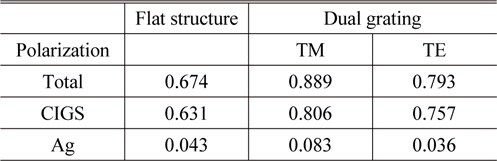
    First, we used the PSO algorithm to optimize the dual grating structure (Fig. 5 (a)) under TM polarization only. The optimized geometry parameters are as follows; HCIGS = 52 nm, P = 300 nm, GCIGS = 70 nm, WCIGS = 145 nm, GAg = 27 nm, WAg = 220 nm, and S = 74 nm. The corresponding absorption efficiency in Fig. 5(b) shows ultra broadband enhancement. An important fact is that the absorption capability of CIGS, as the most active medium, is comparatively much lower at longer wavelengths [7], and thus effective light trapping mechanism is required to achieve high absorption performance, which plasmonic modes are capable of. Indeed, in our optimized structure, three of four absorption peaks pertaining to broadband absorption enhancement are attributed to SPP modes excited at longer wavelength ranges. We present here the total absorption spectrum, including metal absorption (black solid line in the Fig. 5(b)). These SPP modes cause strong field confinement at the interface between Ag and CIGS, as shown in Fig. 5(d), 5(e), and 5(f). The other corresponds to waveguide mode (Fig. 5(c)). In the Table 1, the net absorption efficiency is A = 85.6% for TM polarization, which indicates improvement of 35.4% compared to an optimized flat structure.

    [TABLE 1.] Net absorption efficiency of PSO optimization dual grating structure optimized for TM polarization

    label

    Net absorption efficiency of PSO optimization dual grating structure optimized for TM polarization

       4.2. PSO Optimization of Simultaneous TE and TM Polarized Performance

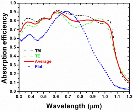
    Next, we applied the PSO algorithm to optimize the dual grating structure under non-polarization, in other words, we consider the average of the net absorption under TE and TM polarization as the fitness function for the PSO algorithm. The optimized geometry has HCIGS = 39 nm, P = 570 nm, GCIGS = 70 nm, WCIGS = 131 nm, GAg = 18 nm, WAg = 129 nm, and S = 187 nm. The optimized net absorption efficiency of 78.1% corresponds to improvement of 23.5% compared to flat structure as seen in Table 2. The absorption performance is somewhat smaller than the only TM optimized case with A = 85.6%. This means that all of the design goals cannot reach optimal values simultaneously due to introducing of additional optimization goals to a system with the same limited number of degrees of freedom. The PSO algorithm is designed to find a trade-off between TE and TM performance, and thus the result is no longer simple to analyze due to the complex coupling of the different modes supported, unlike the TM optimized structure. Therefore, absorption peaks are no longer well-defined and well-spaced for both TM and TE polarizations. Fig. 6(a) indicates absorption spectra for the optimized dual grating and optimized flat structures.

    [TABLE 2.] Net absorption efficiency of PSO optimization dual grating structure optimized for both TM and TE polarizations

    label

    Net absorption efficiency of PSO optimization dual grating structure optimized for both TM and TE polarizations

    A design with larger number of degrees of freedom would be more capable of fully optimizing such a system. Specifically, in order to realize a structure with four well-defined and well-spaced absorption peaks under both TE and TM polarizations, a system with more degrees of freedom would be required. One might note that it is possible to realize such a system in 2D asymmetrical dual grating [24], meanwhile, in such large numbers of optimization parameters, any kind of brute force parametric scanning would not be practical at all.

    In practical applications, the short circuit current density is one of the popular indicators of solar cell performance in terms of optical absorption, assuming that each absorbed photon creates an electron-hole pair that gets collected. In this work, we expressed the short circuit current density (
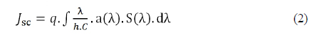
Jsc) as below:

    image

    where, q is the electron charge, λ is the wavelength of incident light, h is the Planck’s constant and C is the velocity of light in vacuum.

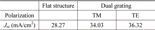
    The short circuit current density of the PSO optimization dual grating structure and the flat structure with the equal volume of CIGS is shown in the Table 3. In the case of TE polarization, the Jsc of PSO optimization dual grating structure is improved over 20% in comparison to the flat structure and for TM polarization the Jsc is improved over 28%. The overall (average) improvement is 24% compared to the flat structure.

    [TABLE 3.] Short circuit current density Jsc of of PSO optimization dual grating structure optimized for both TM and TE polarizations

    label

    Short circuit current density Jsc of of PSO optimization dual grating structure optimized for both TM and TE polarizations

       4.3. Sensitivity

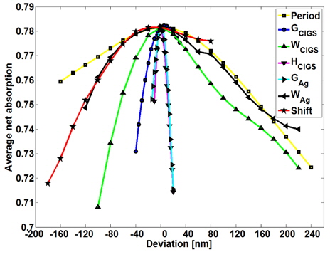
    In practical device fabrication, some geometry parameters may not match with optimized parameters. In order to investigate the effective tolerance of geometry parameters, we examined the sensitivity of absorption performance to varying geometry parameters around the optimal condition (Fig. 7). The optimized structure is rather insensitive to deviations of its design parameters. For P, WCIGS , WAg and S, an error of 20 nm results in a reduction in the averaged net absorption of less than 0.3% compared with optimal value. For GCIGS, GAg and HCIGS, an error of 5 nm results in a reduction in the average net absorption of 0.8%. In fabrication, these tolerances of our optimized design structure are suitable with nanofabrication equipment [25].

    V. CONCLUSION

    In conclusion, we investigated the optimization capability of PSO in thin film CIGS solar cell with dual gratings (composed of top dielectric and bottom metal gratings). The optimized structure produces strong and ultra broadband absorption in the range of 300~1200 nm. PSO algorithm allows the formation of well-spaced and well-defined absorption peaks, as the results of a combination of SPPs and photonic modes induced by metal and dielectric gratings. The potential of PSO is strikingly useful in structure with the larger number of degree of freedom, meanwhile conventional optimization method such as parametric scan requires a prohibitive calculation time. Under only TM and both polarization, the PSO optimized net absorption of A = 85.6% and 78.1%, correspond to ~35.4% and ~23.5% improvement compared to flat structure, respectively. The average improvement of both polarization of the optimized structure in term of the short circuit current density Jsc with respect to the flat structure is 24%.

참고문헌
  • 1. Schock H. W., Noufi R. 2000 “CIGS-based solar cells for the next millennium,” [Prog. Photovolt: Res. Appl.] Vol.8 P.151-160 google
  • 2. Romeo A., Terheggen M., Abou-Ras D., Batzner D. L., Haug F.-J., Kalin M., Rudmann D., Tiwari A. N. 2004 “Development of thin-film Cu(In,Ga)Se2 and CdTe solar cells,” [Prog. Photovol: Res. Appl.] Vol.12 P.93-111 google cross ref
  • 3. Chiril? A., Buecheler S., Pianezzi F., Bloesch P., Gretener C., Uhl A. R., Fella C., Kranz L., Perrenoud J., Seyrling S., Verma R., Nishiwaki S., Romanyuk Y., E., Bilger G., Tiwari A. N. 2011 “Highly efficient Cu(In,Ga)Se2 solar cells grown on flexible polymer films,” [Nat. Mater.] Vol.10 P.857-861 google cross ref
  • 4. Nakada T. 2012 “CIGS-based thin film solar cells and modules: Unique material properties,” [Electron. Mater. Lett.] Vol.8 P.179-185 google cross ref
  • 5. Jackson P., Hariskos D., Lotter E., Paetel S., Wuerz R., Manner R., Wischmann W., Powalla M. 2011 “New world record efficiency for Cu(In,Ga)Se2 thin-film solar cells beyond 20%,” [Prog. Photovolt: Res. Appl.] Vol.19 P.894-897 google cross ref
  • 6. Alonso M. I., Garriga M., Durante Rincon C. A., Hernandez E., Leon M. 2002 “Optical functions of chalcopyrite CuGaxIn1-xSe2 alloys,” [Appl. Phys. A] Vol.74 P.659-664 google cross ref
  • 7. Paulson P. D., Birkmire R. W., Shafarman W. N. 2003 “Optical characterization of CuIn1-xGaxSe2 alloy thin films by spectroscopic ellipsometry,” [J. Appl. Phys.] Vol.94 P.879-888 google cross ref
  • 8. Pillai S., Green M, A. 2010 “Plasmonics for photovoltaic applications,” [Sol. Energy Mater. Sol. Cells] Vol.94 P.1481-1486 google cross ref
  • 9. Panoiu N. C., Osgood Jr R. M. 2007 “Enhanced optical absorption for photovoltaics via excitation of waveguide and plasmon-polariton modes,” [Opt. Lett.] Vol.32 P.2825-2827 google cross ref
  • 10. Pala R. A., White J., Barnard E., Liu J., Brongersma M. L. 2009 “Design of plasmonic thin-film solar cells with broadband absorption enhancements,” [Adv. Mater.] Vol.21 P.3504-3509 google cross ref
  • 11. Atwater H. A., Polman A. 2010 “Plasmonics for improved photovoltaic devices,” [Nat. Mater.] Vol.9 P.205-213 google cross ref
  • 12. Wang W., Wu S., Reinhardt K., Lu Y., Chen S. 2010 “Broadband light absorption enhancement in thin-film silicon solar cells,” [Nano Lett.] Vol.10 P.2012-2018 google cross ref
  • 13. Chriki R., Yanai A., Shappir J., Levy U. 2013 “Enhanced efficiency of thin film solar cells using a shifted dual grating plasmonic structure,” [Opt. Express] Vol.21 P.A382-A391 google cross ref
  • 14. Schuster C. S., Kowalczewski P., Martins E. R., Patrini M., Scullion M, G., Liscidini M., Lewis L., Reardon C., Andreani L. C., Krauss T. F. 2013 “Dual gratings for enhanced light trapping in thin-film solar cells by a layer-transfer technique,” [Opt. Express] Vol.21 P.A433-A438 google cross ref
  • 15. Abass A., Le K. Q., Alu A., Burgelman M., Maes B. 2012 “Dual-interface gratings for broadband absorption enhancement in thin-film solar cells,” [Phys. Rev. B] Vol.85 P.115449 google cross ref
  • 16. Ferry V. E., Polman A., Atwater H. A. 2011 “Modeling light trapping in nanostructured solar cells,” [ACS Nano] Vol.5 P.10055-10064 google cross ref
  • 17. Eberhart R., Kennedy J. 1995 “Particle swarm optimization,” [Proc. IEEE International Conf. on Neural Networks] Vol.4 P.1942-1948 google
  • 18. Saremi M. S., Magnusson R. 2007 “Particle swarm optimization and its application to the design of diffraction grating filters,” [Opt. Lett.] Vol.32 P.894-896 google cross ref
  • 19. Mutitu J. G., Shi S., Chen C., Creazzo T., Barnett A., Honsberg C., Prather D. W. 2008 “Thin film silicon solar cell design based on photonic crystal and diffractive grating structures,” [Opt. Express] Vol.16 P.15238-15248 google cross ref
  • 20. Magnusson R., Saremi M. S., Johnson E., G. 2010 “Guidedmode resonant wave plates,” [Opt. Lett.] Vol.35 P.2472-2474 google cross ref
  • 21. Palik E. D. 1985 Handbook of Optical Constants of Solids google
  • 22. Chriki R. 0000 “Enhanced efficiency of thin film solar cells using a shifted dual grating plasmonic structure,” google
  • 23. Roy S., Subramaniam P. C. 1992 “TE-polarized surface plasmon polaritons in metal waveguides bounded by selffocusing and self-defocusing media,” [Opt. Lett.] Vol.17 P.911-913 google cross ref
  • 24. Yu Z., Raman A., Fan S. 2010 “Fundamental limit of light trapping in grating structures,” [Opt. Express] Vol.18 P.A366-A380 google cross ref
  • 25. Vieu C., Carcenac F., Pepin A., Chen Y., Mejias M., Lebib A., Manin-Ferlazzo L., Couraud L., Launois H. 2000 “Electron beam lithography: resolution limits and applications,” [Appl. Surf. Science] Vol.164 P.111-117 google cross ref
OAK XML 통계
이미지 / 테이블
  • [ FIG. 1. ]  The flowchart of the PSO algorithm.
    The flowchart of the PSO algorithm.
  • [ ] 
  • [ FIG. 2. ]  Net absorption efficiency as the function of thickness of flat structure.
    Net absorption efficiency as the function of thickness of flat structure.
  • [ FIG. 3. ]  (a) Schematic diagram of bottom grating structure. (b) Absorption efficiency spectra of optimized bottom grating structure for normal incidence light (black dashed line for TM, green dashed line for TE, red solid line for average of TM and TE polarizations) and optimized flat structure (blue triangle lines). (c-d) Magnetic field distributions for TM polarization at λ = 560 nm and λ = 740 nm, respectively. (e) Electric field distribution for TE polarization at λ = 640 nm. The optimized structure parameters are HCIGS = 40 nm, PAg = 400 nm, WAg = 120 nm and GAg = 20 nm. The average net absorption is A = 66.8%.
    (a) Schematic diagram of bottom grating structure. (b) Absorption efficiency spectra of optimized bottom grating structure for normal incidence light (black dashed line for TM, green dashed line for TE, red solid line for average of TM and TE polarizations) and optimized flat structure (blue triangle lines). (c-d) Magnetic field distributions for TM polarization at λ = 560 nm and λ = 740 nm, respectively. (e) Electric field distribution for TE polarization at λ = 640 nm. The optimized structure parameters are HCIGS = 40 nm, PAg = 400 nm, WAg = 120 nm and GAg = 20 nm. The average net absorption is A = 66.8%.
  • [ FIG. 4. ]  (a) Schematic diagram of top grating structure. (b) Absorption efficiency spectra of optimized top grating structure for normal incidence light (black dashed line for TM, green dashed line for TE, red solid line for average of TM and TE polarizations) and optimized flat structure (blue triangle line). (c-d) Magnetic field distributions for TM polarization at λ = 770 nm and λ = 1110 nm, respectively. (e) Electric field distribution for TE polarization at λ = 985 nm. The optimized structure parameters are HCIGS = 40 nm, PCIGS = 600 nm, WCIGS = 180 nm and GCIGS = 70 nm. The average net absorption is A = 73.35%.
    (a) Schematic diagram of top grating structure. (b) Absorption efficiency spectra of optimized top grating structure for normal incidence light (black dashed line for TM, green dashed line for TE, red solid line for average of TM and TE polarizations) and optimized flat structure (blue triangle line). (c-d) Magnetic field distributions for TM polarization at λ = 770 nm and λ = 1110 nm, respectively. (e) Electric field distribution for TE polarization at λ = 985 nm. The optimized structure parameters are HCIGS = 40 nm, PCIGS = 600 nm, WCIGS = 180 nm and GCIGS = 70 nm. The average net absorption is A = 73.35%.
  • [ FIG. 5. ]  PSO optimization of TM polarized performance. (a) Schematic diagram of optimized dual grating structure. (b) Absorption efficiency spectra of optimized dual grating structure for normal incidence light (black dashed line for TM, green dashed line for TE, black solid line for total absorption of TM, red solid line for average of TM and TE polarizations) and optimized flat structure (blue triangle lines). (c-f) Magnetic field profiles under TM illumination at absorption peak wavelengths, (c) λ = 365 nm, (d) λ = 650 nm, (e) λ = 900 nm, and (f) λ = 1090 nm, respectively. The optimized structure parameters are HCIGS = 52 nm, P = 300 nm, GCIGS = 70 nm, WCIGS = 145 nm, GAg = 27 nm, WAg = 220 nm, and S = 74 nm. The average net absorption is A = 85.6%.
    PSO optimization of TM polarized performance. (a) Schematic diagram of optimized dual grating structure. (b) Absorption efficiency spectra of optimized dual grating structure for normal incidence light (black dashed line for TM, green dashed line for TE, black solid line for total absorption of TM, red solid line for average of TM and TE polarizations) and optimized flat structure (blue triangle lines). (c-f) Magnetic field profiles under TM illumination at absorption peak wavelengths, (c) λ = 365 nm, (d) λ = 650 nm, (e) λ = 900 nm, and (f) λ = 1090 nm, respectively. The optimized structure parameters are HCIGS = 52 nm, P = 300 nm, GCIGS = 70 nm, WCIGS = 145 nm, GAg = 27 nm, WAg = 220 nm, and S = 74 nm. The average net absorption is A = 85.6%.
  • [ TABLE 1. ]  Net absorption efficiency of PSO optimization dual grating structure optimized for TM polarization
    Net absorption efficiency of PSO optimization dual grating structure optimized for TM polarization
  • [ FIG. 6. ]  PSO optimization of dual grating structure for both TM and TE polarizations. (a) Absorption efficiency spectra of optimal dual grating structure for normal incidence light (black dashed line for TM, green dashed line for TE, red solid line for average of TM and TE polarizations) and optimized flat structure (blue triangle lines).
    PSO optimization of dual grating structure for both TM and TE polarizations. (a) Absorption efficiency spectra of optimal dual grating structure for normal incidence light (black dashed line for TM, green dashed line for TE, red solid line for average of TM and TE polarizations) and optimized flat structure (blue triangle lines).
  • [ TABLE 2. ]  Net absorption efficiency of PSO optimization dual grating structure optimized for both TM and TE polarizations
    Net absorption efficiency of PSO optimization dual grating structure optimized for both TM and TE polarizations
  • [ ] 
  • [ TABLE 3. ]  Short circuit current density Jsc of of PSO optimization dual grating structure optimized for both TM and TE polarizations
    Short circuit current density Jsc of of PSO optimization dual grating structure optimized for both TM and TE polarizations
  • [ FIG. 7. ]  Examining the sensitivity of PSO optimization of dual grating structure optimized for both TM and TE polarizations. Examined parameters: Period (yellow line), CIGS grating thickness (blue line), CIGS grating width (green line), CIGS layer thickness (pink), Silver grating thickness (magenta line), silver grating thickness (black line) and shift between two gratings (red line).
    Examining the sensitivity of PSO optimization of dual grating structure optimized for both TM and TE polarizations. Examined parameters: Period (yellow line), CIGS grating thickness (blue line), CIGS grating width (green line), CIGS layer thickness (pink), Silver grating thickness (magenta line), silver grating thickness (black line) and shift between two gratings (red line).
(우)06579 서울시 서초구 반포대로 201(반포동)
Tel. 02-537-6389 | Fax. 02-590-0571 | 문의 : oak2014@korea.kr
Copyright(c) National Library of Korea. All rights reserved.