Optical interconnect technology is receiving a great amount of research and development efforts as the need for higher-bandwidth serial interfaces are continuously increasing and the conventional electrical interconnect technology is facing serious bandwidth, power, and footprint limitations. Initial efforts in optical interconnect implementation have been based on heterogeneous integration of photonic components realized in III-V compound semiconductors and Si electronics [1]. However, realization of photonic devices in Si processing technology has become possible and high-performance Si modulators [2] and Ge photodetectors on Si [3] are now available. Furthermore, several electronic-photonic integrated circuits based on the silicon platform have been reported [4-6].
Si photonic systems can be realized either in the hybrid or monolithic manner as each offers its own advantages and disadvantages [7, 8]. Monolithic integration minimizes parasitic components but requires complicated processing technology in order to realize both photonic devices and electronic circuits on the same wafer. Hybrid integration decouples electronic circuits with photonic devices and takes advantage of utilizing separately optimized processing technologies but usually suffers from parasitic effects and complicated packaging issues. This paper reports our efforts of realizing a hybrid integrated optical transmitter composed of a Si ring modulator and CMOS driver circuits. The ring modulator is fabricated with 220-nm Si-oninsulator (SOI) process and the driver circuits with 65-nm CMOS technology. They are hybrid integrated on a printed circuit board with bonding wires. With careful design optimization, the bonding-wire inductance is used for enhancing driver bandwidth. 25-Gb/s operation is successfully demonstrated with our optical transmitter.
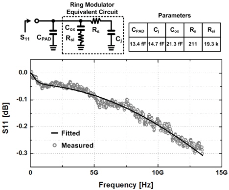
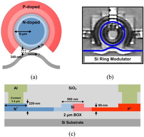
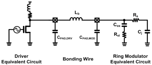
Figure 1(a), (b) and (c) show the structure, microphotograph and cross-section of the ring modulator used in this work, respectively. It consists of a ring waveguide having 8 μm radius and a bus waveguide. The coupling gap is 0.34 μm. The waveguide width is 500 nm and is realized with 220-nm Si on 2-μm buried oxide layer. The light signal goes into and comes out of the modulator through grating couplers. The device fabrication is done with IME Si-photonics foundry service through OpSIS. For modulator operation, the effective group index of the ring waveguide is modulated by the reverse voltage applied to the PN junction in the ring waveguide. Figure 2 shows the equivalent circuit model of our ring modulator [9]. Cox, Cj, Rs and Rsi represent the capacitance through the buried oxide layer, of the reverse-biased PN junction, diode series resistance and resistance through the Si substrate, respectively. CPAD represents the parasitic capacitance of the signal pad used for measurement. The numerical value of each component is determined by fitting the simulation result to measured electrical S11 data as shown in Fig. 2.
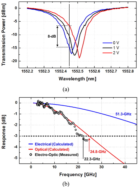
The measured optical transmission characteristics of the ring modulator at different reverse bias voltages are shown in Fig. 3(a). The resonance wavelength red shifts with the increasing reverse bias voltage as the effective group index of the ring waveguide increases with the reverse bias voltage. The modulation efficiency of our modulator is 20 pm/V and the estimated ring quality factor (Q) is 7800. With input wavelength of 1552.45 nm and the reverse bias voltage changing from 0 to 2 V, our modulator achieves extinction ratio of 8 dB.
The modulation bandwidth of a ring modulator is limited by cavity photon lifetime (τ
III. CMOS DRIVER AND ON-CHIP PRBS GENERATOR
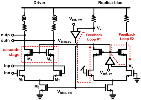
Figure 4 shows the schematic of the modulator driver and replica-bias circuit. Our modulator driver uses 3-V supply so that it can provide 2-V driving voltage to the ring modulator for achieving the sufficient extinction ratio. Since high supply voltages can threaten transistor reliability, we use the current mode logic (CML) topology in a cascode stage. Transistors having low threshold voltages (M1 and M2) are used in the input stage in order to maximize the transition speed. In the cascode stage, thick-gate transistors (M3 and M4) are used in order to withstand the overdrive voltage. Since the use of thick-gate transistors in the cascode stage limits the bandwidth of the modulator driver, shunt-peaking inductors are used for bandwidth extension. The replica-bias circuit consists of two feedback loops, one for controlling the output swing and the other for regulating overdrive-voltage. Each of two feedback loops forces Vx to be equal to Vref,sw and Vy to Vref,ov, respectively. With 1-V Vref,sw and 1.2-V Vref,ov, the modulator driver output swing is fixed at 2 V and the modulator driver input stage has VDS fixed at 1.2 V.
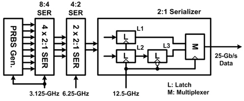
An on-chip pseudo-random binary sequence (PRBS) generator is integrated with the driver circuit. Figure 5 shows the structure of PRBS generator. A parallel PRBS generator [11] having eight channels of 3.125-Gb/s data is custom designed and serialized throughout three 2:1 serializer stages, each of which is a double-edge triggered flip-flop with an additional latch for half-rate delay, for producing 25-Gbps PRBS data. Such an internal PRBS generator allows simple transmitter testing configuration.
IV. HYBRID INTEGRATION OF OPTICAL TRANSMITTER
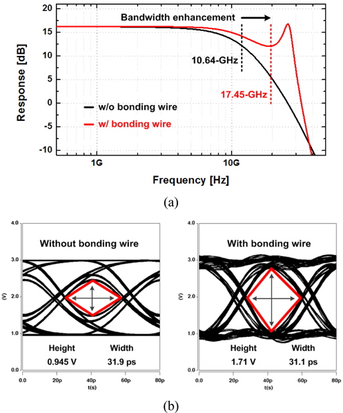
Figure 6 shows the equivalent circuit model of our hybrid-integrated optical transmitter. The driver circuit is simply represented by a common-source amplifier. The pad capacitance for the driver, CPAD,DRV, and for the ring modulator, CPAD,MOD, significantly limit the driver bandwidth. However, adding a series inductor can provide a significant amount of bandwidth enhancement [12]. In our configuration, the bonding wire provides the necessary series inductance. Figure 7(a) and (b) show the simulated frequency response and the eye diagram with and without the bonding wire inductance. For the simulation, CPAD,DRV of 60 fF estimated from the pad size of 90-μm x 60-μm, and CPAD,MOD of 13.4 fF determined from the measurement as explained above are used. CPAD,MOD is smaller than CPAD,DRV because its size (60-μm x 60-μm) is smaller and it is made on Si on the insulator. In addition, the bonding wire inductance of 1 nH is used. As can be seen in the figure, we observed that the bonding wire enhances driver bandwidth from 10.64 GHz to 17.45 GHz and the resulting vertical eye opening is enhanced from 0.945 V to 1.71 V. A small amount of horizontal eye opening degradation is due to the frequency peaking caused by the series inductance.
V. DEMONSTRATION OF OPTICAL TRANSMITTER
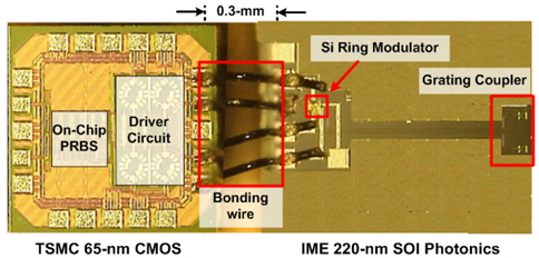
Figure 8 shows a microphotograph of the hybrid-integrated optical transmitter with bonding wires. For this, the CMOS driver circuit and Si ring modulator are fixed on the printed circuit board and wedge bonded using aluminum wires. Four bonding wires are used for the integration, one for the signal and others for ground connection. The total length of the bonding wire is approximately 1 mm and the resulting bonding-wire inductance is 1 nH [13].
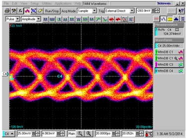
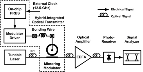
Figure 9 describes the experimental setup used for our transmitter demonstration. An Agilent 81689A tunable laser provides -5 dBm input light at 1552.45 nm into the grating coupler. A polarization controller (PC) is used to minimize the insertion loss as the grating coupler is polarization dependent. The erbium-doped fiber amplifier (EDFA) is used to amplify the modulator output light. The modulated optical signal is converted to the electrical signal using a Newport 1414 25-GHz photoreceiver and observed with a Tektronix CSA8000B signal analyzer. An on-chip PRBS generator operates with an external 12.5-GHz clock. The measured eye diagram of our transmitter for 25-Gb/s 231-1 PRBS data is shown in Fig. 10. With the driver having 2-Vpp output swing, no error is observed for more than an hour. The driver circuit consumes 120-mW at 3-V supply and the on-chip PRBS generator consumes 60-mW at 1.2-V supply.
We present an optical transmitter based on Si ring modulator and CMOS driver circuit. The bonding wire between the modulator and the driver is used for its simplicity and cost-effectiveness. In addition, with careful design optimization, the bonding wire is used to enhance the driver bandwidth and, consequently, provide a better eye diagram.