In recent years, the n-type and p-type doping control of ZnO NWs has attracted considerable attention. Especially, ZnO-based NWs are useful due to their manageable conductance with doping control in addition to their large length-to-diameter and surface-to-volume ratio compared to the bulk and films of ZnO [1]. Futhermore, ZnO-based semiconductor materials have been given much attention due to their excellent electrical and optical characteristics, such as large band gap energy of 3.37 eV and large exciton binding energy of 60 meV at room temperature (RT) [2].
Until now, few reports have been presented on the study of the opptical properties of Ga doped and Ag doped ZnO NW measured at low temperature to investigate doping effect. Doping in NWs can create defects that play a role as donor or acceptor sites resulting in changes to the electrical conductivity [3].
In this article, pristine ZnO, 3 wt.% Ga-doped (3GZO), and 3 wt.% Ag-doped (3SZO) ZnO NWs have been synthesized using the hot-walled pulse laser deposition (HW-PLD) technique. The optical and chemical properties of the doped ZnO NWs were characterized by SEM/EDX, PL, and XPS. Especially, low temperature PL could clearly verify the doping effect on ZnO NWs.
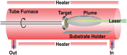
ZnO-based NWs are synthesized using the HW-PLD process with 20 Å Au film as a catalyst on sapphire substrates. HW-PLD has a target rotating system, ensuring homogeneous target ablation as shown in Fig. 1. ZnO, 3GZO, and 3SZO ceramic targets were used when we fabricated the NWs under the optimized conditions in HW-PLD. The diverse ZnO-based NWs were grown in a HW-PLD furnace at the processing temperature of 800℃ with Ar carrier gas. The energy density of the laser is set at 1.2 J/cm2, and the area shot on the target surface is 0.042 cm2. The growth time of ZnO-based NWs is 30 min. During the deposition, the Ar gas flow rate was fixed at 90 sccm and the pressure inside the quartz tube was maintained at 1.2 Torr.
The morphology of the as-grown samples was studied using field emission scanning electron microscopy (FE-SEM) operated at 20 kV. Energy-dispersive X-ray spectroscopy (EDX) analysis of a single NW was then performed. PL was carried out at low temperature (6 K) with He-Cd laser at an excitation wavelength of 248 nm.
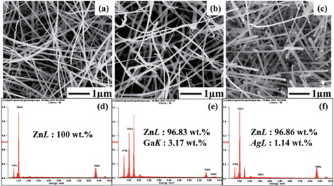
Figures 2(a)~2(f ) show the controlled morphology of the ZnO, 3GZO, 3SZO NWs, and EDX spectra. Using SEM with EDX (SEM/EDX) is an electron probe microanalysis method that has been used extensively to characterize the size, morphology, and elemental composition of samples. The NWs have thread-like shapes and an Au nanoparticle at the end of each NW is clearly observed. It is understood that the nanoparticle is an Au catalyst that initiates the growth of the NWs by HW-PLD, which is a vapor-liquid-solid (VLS) mechanism. The catalyst can be identified by tips that are brighter than the stem parts of the NWs. As can be seen in the figure, the orientation and the distribution of the NWs are random with the diameter of about 100 nm and the length of about 1 μm. ZnO based NWs were synthesized with ZnO targets by HW-PLD. Figures 1(a)~1(c) show the top view of the FE-SEM images of ZnO-based NWs with pure ZnO, 3GZO, and 3SZO with 20 Å Au film as a catalyst. As shown in Fig. 2, many ramdom direction ZnO based NWs with a mean dimeter of abut 70 nm and an average length of about 9 μm were obtained at 800℃.
The EDX analysis yields reasonably accurate quantitative results featuring all the elements present in the tested compounds, namely C, O, N, Na, S, Al, Si, and Cl. Furthermore, the carbon film has very low backscattered electron (BSE) yield compared to that from the particle. Therefore, in the BSE mode, the particle image is seen with very high contrast. This greatly improves the quality and speed of the automated mapping of particles by SEM prior to EDX analysis [4]. Figures 2(d)~2(f) show backscatter electron images of the morphology and surface composition of the fractured surface of a specimen, which correspond to the EDX spectrum. ZnO, Ag, and Ga were clearly observed. The EDX spectrum revealed the presence of Zn, Ga, and Ag elements. HW-PLD is a well established growth method for oxide thin films and nanostructures of high structural quality. Therefore, HW-PLD is a simple synthesis process and only target control can give an effective doping in the ZnO NWs. This result indicates that the impurities were doped well in the ZnO based NWs. According to the study in terms of Ag doping, it is considered that the irregularity of the heavily doped samples stems from the lattice stress induced by the substitution of Ag with Zn [5]. Unlike pure ZnO NWs, the 3SZO NW has many defects originating from the accumulated stress caused by the doping. Near the surface of the NW, many edge dislocations are found to support the dopinginduced stress. The NW growth direction is not perpendicular to the primary planes in forming the deviation from the upright ABABA stacking, implying a switch of the primary growth plane [6]. This means it is not easy to dope Ag with ZnO. Therefore, the EDX spectra of 3SZO revealed that the Ag content is lower than 3 wt.%, even though we used 3 wt.% target as shown in Fig. 2(f ).
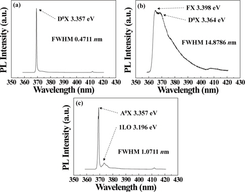
Photoluminescence (PL) analysis is a powerful tool used to investigate Ga and Ag doping in ZnO nanostructures because it can give the band gap as well as the defect information of the doped semiconductor nanosutructures non-destructively [7]. Figure 3 shows the low-temperature PL spectra of the pure ZnO, 3GZO, and 3SZO by excitation of a 325 nm He-Cd laser. The measured temperature is decreased to 6 K to avoid the screening effect of the phonon vibration scattering on the original luminescence, which can interrupt the emission of the dopant sites. At room temperature, it is difficult to distinguish each PL peak origin due to phonon vibration. We could observe the major peaks, a nearband- edge (NBE) emission, and VO-related PL emission. The spectra of all samples show narrow UV emission peaks. The UV emission originated from the near-band-edge (NBE) peak that is responsible for the recombination of free excitons of ZnO [8]. From the spectra data, the undoped ZnO NW shows a strong and narrow NBE emission at 369.21 nm, while the UV emission peaks from 3GZO and 3SZO are 366.95 nm and 368.94 nm, repectively. In the case of 3GZO and 3SZO NWs, the center photon energy of the NBE emissions is shifted to a low energy direction using the Burstein Moss effect as follows [9]:

where ΔEBN is the widened energy bandgap and n is the doping concentration. It is well known that, when ZnO is doped with Ga and Ag elements, the excess carriers supplied by the impurities contribute to the enhancement of the electrical conductivity of the ZnO nanostructures [10]. In Fig. 3(b), it is clearly observed that the donor-bound exciton peak (D0X) is dominant due to the doping of Ga into ZnO while the acceptor-bound exciton (A0X) peak is found in 3SZO NWs, measured at a low temperature of 6K as shown in Fig. 3(c). Since the substitution of Ag ions into the Zn sites can compensate for the extra electrons generated by oxygen vacancies, the donor-bound emissions are well suppressed by Ag-doping. Also, a longitudinal optical (LO) phonon replica of the free exciton peak is observed. The PL data of 3SZO are compared with those of pristine ZnO and 3GZO NWs to support opti- cally p-type NWs by observing the acceptor-bound peak.
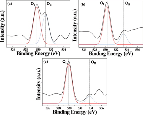
XPS analysis was used to identify the change of chemical structure caused by Ga and Ag-doping in the ZnO NWs. Figure 4 shows the XPS spectra of ZnO, 3GZO, and 3SZO NWs. Generally, a typical O1s peak in the surface can be consistently fitted with three nearly Gaussians, centered at 529.77 eV, 530.27 eV, and 529.91 eV, respectively. The low binding energy component (OI) is from the O2- ions wurtzite structure of the hexagonal Zn2+ ion array, surrounded by Zn (or the substitution of Ga) atoms [11]. The component on the low binding energy (OI) side of the O1s spectrum at 529.77 eV can be attributed to O2- ions surrounding surrounded by the Zn, Ga, and Ag in the atoms [12]. The density of this component is a measure of the number of oxygen atoms in a fully oxidized stoichiometric atmosphere. The binding energy component (OII) centered at 531.14 eV is associated with O2- ions that are in oxygen-deficient regions. Generally, (OII) related-oxygen vacancies supply free electron carriers in the film, resulting in the increase of electron concentration [13,14]. It is important to note that the change of the area of the oxygen vacancy related peak can demonstrate the successful doping.
In summary, we fabricated pristine ZnO, Ga(3 wt.%)-doped (3GZO), and Ag(3 wt.%)-doped (3SZO) ZnO nanowires (NWs) using HW-PLD. The doping of Ga and Ag in ZnO NWs was observed by analyzing the optical and chemical properties. Low temperature PL was performed to observe the optical property of doped NWs to avoid the screening effect of the phonon vibration scattering on the original luminescence. A strong donor-bound exciton peak was found in 3 GZO NWs while the acceptor-bound exciton peak was found in the 3SZO NWs. X-ray photoelectron spectroscopy (XPS) also indicated that the shift of binding energy was mainly attributed to the interaction between the metal ion and ZnO NWs. Note that the donor-bound exciton peak and acceptor bound exciton peaks clearly demonstrate the successful doping in 3GZO NWs and 3SZO NWs, respectively.