검색 전체 메뉴
PDF
맨 위로
OA 학술지
Design and Performance Analysis of a Multi Wavelength Terahertz Modulator Based on Triple-Lattice Photonic Crystals
  • 비영리 CC BY-NC
  • 비영리 CC BY-NC
ABSTRACT
Design and Performance Analysis of a Multi Wavelength Terahertz Modulator Based on Triple-Lattice Photonic Crystals
KEYWORD
Multi-wavelength , Photonic crystal , THz wave , Triple lattice , Modulator
  • I. INTRODUCTION

    Nowadays the demand for broadband data communication is growing rapidly, owing to the information explosion. Optical communications systems have been researched for a long time, and the study of THz communications systems has become an inevitable trend. The THz modulator is one of the key devices in a THz communications system. Recently, there has been growing interest in studying THz wave modulators, especially multi wavelength THz modulators [1-3]. Currently dual-wavelength and four-wavelength THz modulators based on a compound-lattice photonic crystal (PC) have been proposed [4, 5]. A novel type of six-wavelength THz modulator based on a triple-lattice photonic crystal is proposed in this paper.

    As is well known, various methods may be used to realize THz wave modulation [6, 7]. The PC material plays an important role in a THz modulator because of its excellent characteristics and production technology [8, 9]. A PC has the characteristics of a photonic band gap (PBG) and photon localization [10, 11]. A high-efficiency, controllable multi wavelength photonic crystal modulator can be fabricated by using a PC with defects. Using the disappearing-defect-mode theory, we have designed a six-wavelength THz modulator that has the advantages of high extinction ratio and low insertion loss.

    II. MODULATION MECHANISM

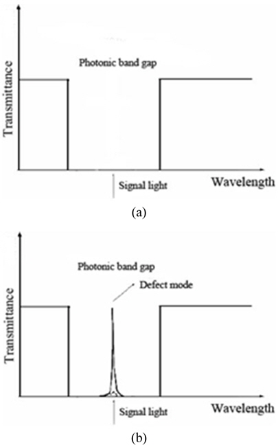
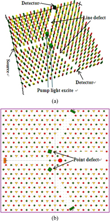
    Defect-mode disappearance is based on the photon-localization characteristic of a PC. This characteristic of a PC is due to the combination of both point and line defects. Line defects are introduced as waveguides to transmit THz wave with frequencies located in the PBG, while point defects are used as resonant cavities, in which only THz frequencies in accord with the resonant frequency (or defect-mode frequency) can be selected. Figure 1 is a schematic diagram of the modulation based on defect-mode disappearance. When the point defects are filled with a tunable material and the pump light is applied to the point defects, the refractive index of the material will change and the defect modes of the point defects will disappear. Therefore, the input THz wave cannot resonate in the cavity and the modulator is in the “off” state, as shown in Fig. 1(a). However, if there is no pump light, the THz wave will resonate in the cavity and the modulator is in the “on” state, as shown in Fig. 1(b) [12, 13].

    III. STRUCTURAL DESIGN AND PERFORMANCE ANALYSIS

       3.1. Structural Design

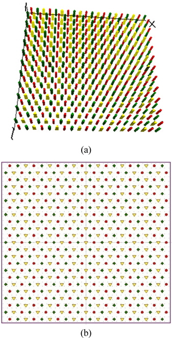
    A triple-triangular-lattice PC is composed of three triangular-lattice photonic crystals, including circular, square, and triangular dielectric cylinders. Figure 2 shows the lattice structure of the PC. Its structural parameters are: lattice constant a = 92 μm, radius of circular dielectric cylinders r = 13.9393 μm, width of square dielectric cylinders w= 25.0909 μm, rotation angle of square dielectric cylinders θ= 45°, base length of triangular dielectric cylinders w' = 41.8181 μm, and height of triangular dielectric cylinders h = 30.6666 μm. The material of the dielectric cylinders is silicon (Si) with refractive index n1 = 3.418 in the THz region. The substrate material is air with refractive index n2 = 1.

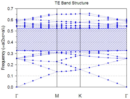
    The band structure of this triple-triangular-lattice PC for TE waves, as calculated by the plane-wave method (PWM), is shown in Fig. 3.

    The shaded part in Fig. 3 is the PBG. The normalized frequency a/λ of the PBG is 0.326-0.522, corresponding to wavelengths of 176.24-282.2 μm. The width of the PBG is 0.196, which is much wider than that of a compound-lattice structure [4, 5].

    To achieve multi wavelength modulation, two point defects and two line defects are introduced into the photonic crystal at the same time, as shown in Fig. 4. The point defects and line defects are directly coupled.

    The tunable material used in the point defects is gallium arsenide (GaAs), for which the THz refractive index in the photo-excited condition is complex and defined as N = n - in', where n and n' are the real and the imaginary parts of the refractive index respectively. The complex refractive index N depends on the wavelength and intensity of the external excitation light wave (pump light) [14]. According to the modulation mechanism mentioned above, when the pump (wavelength 810 nm) intensity is 0.4 μJ/cm2, n' of GaAs changes and the defect modes of the point defects disappear. Thus the input THz wave cannot resonate in the cavity and the modulator is in the “off” state. However, if the pump light is absent, the THz wave will resonate in the cavity and the modulator is in the “on” state.

    In Fig. 4 the width of the upper square point defect is w1 = 2.49 w and the rotation angle of the upper point defect is 15°, while the width of the lower square point defect is w1 = 2.49 w and its rotation angle is 35°. The upper and lower line defects used to transmit the beams of the THz wave correspond to the upper and lower point defects respectively. The larger red, circular dielectric cylinder in Fig. 4 is the result of fine tuning used to increase the transmittance of the defect modes of the square point defects.

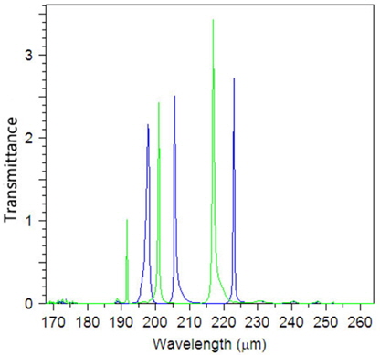
    Figure 5 displays the simulation results for the transmission spectrum. Six beams of the THz wave propagate through the modulator when the modulator is in “on” state, as shown. Each square point defect can modulate three beams of the THz wave. The wavelengths of the three defect modes produced by the upper square point (blue line) are 197.86 μm, 205.64 μm, 222.91 μm respectively. The wavelengths of the three defect modes produced by the lower square point (green line) are 191.67 μm, 200.92 μm, 216.82 μm respectively. The sum of the numbers of defect modes produced by upper and lower square points is six.

       3.2. Performance Analysis

    For the case of the six beams of the THz wave being incident simultaneously, the extinction ratio and insertion loss of the modulator are analyzed in detail below. From Fig. 5, the six incident wavelengths are set as 191.67 μm, 197.86 μm, 200.92 μm, 205.64 μm, 216.82 μm, and 222.91 μm respectively. All of the incident THz waves are Gaussian and continuous.

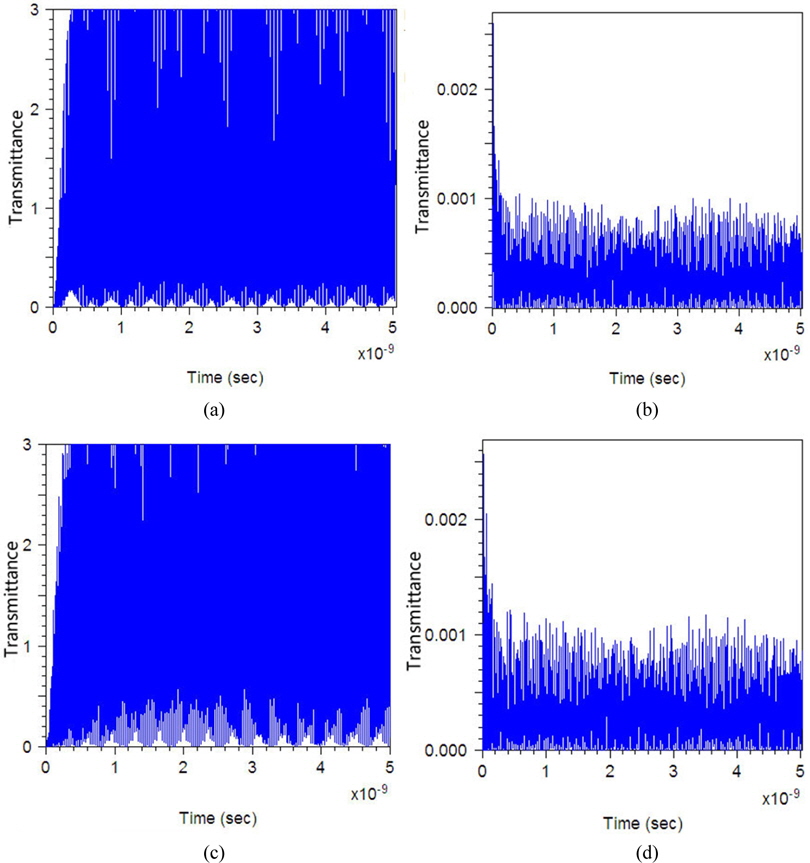
    The extinction ratio is an important index to evaluate the capacity of modulation. The time-domain steady-state response is shown in Fig. 6. As registered by the upper detector in Fig. 4, Figs. 6(a) and 6(b) show the “on” and “off” states of the modulator respectively. As registered by the lower detector in Fig. 4, Figs. 6(c) and 6(d) show the “on” and “off” states of the modulator respectively.

    The definition of extinction ratio is

    image

    where Imax is the maximum transmission intensity of the THz wave after modulation, Imin is the minimum transmission intensity of the THz wave after modulation, and η is the extinction ratio of the modulator. The value of Imax is the sum of the values in Figs. 6(a) and 6(c), while the value of Imin is the sum of the values in Figs. 6(b) and 6(d) respectively. From Fig. 6 we can obtain the value of Imax as 5.8 and the value of Imin as 2.179×10⁻³. From Eq (1), we obtain an extinction ratio of 34.25 dB.

    The definition of insertion loss is

    image

    where Iin is the intensity of the incident THz wave and Imax is the maximum transmission intensity of the THz wave after modulation. The value of Iin is 6, and from Eq (2) we obtain an insertion loss of 0.147 dB.

    The definition of the modulation rate is

    image
    image

    where T is the response time of the system and v is the modulation rate. T is determined by the sum of the response time of GaAs material ㅌ’s change in refractive index (T1) and the stability time of the “on” or “off” state of the modulator (T2). Here T1 is 100 ps [15] and T2 3.2499 ×10⁻¹⁰s from Fig. 6. The modulation rate is 2.35 GHz, as obtained from Eqs. (3) and (4).

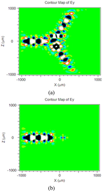
    The steady-state THz wave field intensity distributions of in “on” (n' = 0) and “off” states (n' = 2.55) are shown in Figs. 7(a) and 7(b) respectively.

    Figure 7 shows that the six beams of the THz wave were modulated effectively by the multi-wavelength photonic-crystal THz modulator with a large extinction ratio.

    The simulation results show that this novel multi wavelength photonic-crystal THz modulator can effectively modulate a THz wave, with large extinction ratio and low insertion loss.

    IV. CONCLUSION

    A novel multi wavelength THz modulator based on a triple-triangle-lattice-structure photonic crystal is proposed. By changing the GaAs refractive index, the modulation of six wavelengths (191.67 μm, 197.86 μm, 200.92 μm, 205.64 μm, 216.82 μm, and 222.91 μm) can be realized. The extinction ratio is as large as 34.25 dB, the insertion loss as low as 0.147 dB, and the modulation rate 2.35 GHz. This modulator presents a theoretical foundation for research in communications devices for the THz range, and can also meet the requirements of future THz wave communications systems better.

참고문헌
  • 1. Chen H. M., Su J., Wang J. L., Zhao X. Y. 2011 “Opticallycontrolled high-speed terahertz wave modulator based on nonlinear photonic crystals,” [Opt. Express] Vol.19 P.3599-3603 google cross ref
  • 2. Fekete L., Kadlec F., Nemec H., Kuzel P. 2007 “Fast one-dimensional photonic crystal modulators for the terahertz range,” [Opt. Express] Vol.15 P.8898-8912 google cross ref
  • 3. Nguyen H. C., Sakai Y., Shinkawa M., Ishikura N., Baba T. 2011 “10Gb/s operation of photonic crystal silicon optical modulator,” [Opt. Express] Vol.19 P.13000-13007 google cross ref
  • 4. Li T. D. J., Chen H. M. 2010 “Terahertz wave tunable resonator based on compound lattice photonic crystal,” [Proc. The 9th International Conference on Optical Communication and Networks] P.402-405 google
  • 5. Zhou W., Chen H. M. 2013 “Study on the characteristics of quadruple-wavelength THz modulator based on compound lattice photonic crystal with direct-coupled structure,” [Proc. The 2013 International Conference on Communication Technology] P.821-830 google
  • 6. Rahm M., Li J. S., Padilla W. J. 2013 “THz wave modulators: A brief review on different modulation techniques,” [J. Infrared Milli. Terahz. Waves] Vol.34 P.1-27 google cross ref
  • 7. Figotin A., Godin Y. A., Vitebsky I. 1998 “Two-dimensional tunable photonic crystals,” [Phys. Rev. B] Vol.57 P.2841-2848 google
  • 8. Li J. S., Zouhdi S. 2012 “Ultrafast and low-power terahertz wave modulator based on organic photonic crystal,” [Opt. Commun.] Vol.285 P.953-956 google cross ref
  • 9. Li J. S. 2007 “Terahertz modulator using photonic crystals,” [Opt. Commun.] Vol.269 P.98-101 google cross ref
  • 10. Yablonovitch E. 1987 “Inhibited spontaneous emission in solid-state physics and electronics,” [Phys. Rev. Lett.] Vol.58 P.2059 google cross ref
  • 11. John S. 1987 “Strong localization of photons in certain disordered dielectric super lattices,” [Phys. Rev. Lett.] Vol.58 P.2486 google cross ref
  • 12. Notomi M., Shinya A., Mitsugi S., Kira G., Kuramochi E., Tanabe T. 2005 “Optical bistable switching action of Si high-Q photonic-crystal nanocavities,” [Opt. Express] Vol.13 P.2678-2687 google cross ref
  • 13. Chen T., Liu P., Liu J., Hong Z. 2014 “A terahertz photonic crystal cavity with high Q-factors,” [Appl. Phys. B] Vol.115 P.105-109 google
  • 14. Tiedje H. F., Haugen H. K., Preston J. S. 2007 “Measurement of nonlinear absorption coefficients in GaAs. InP, and Si by an optical pump THz probe technique,” [Opt. Commun.] Vol.274 P.187-197 google cross ref
  • 15. Fekete L., Kadlec F., Kuzel P. 2007 “Ultrafast opto-terahertz photonic crystal modulator,” [Opt. Lett.] Vol.32 P.680-682 google cross ref
OAK XML 통계
이미지 / 테이블
  • [ FIG. 1. ]  Schematic diagram of modulation based on defect-mode disappearance: (a) “off” state, (b) “on” state.
    Schematic diagram of modulation based on defect-mode disappearance: (a) “off” state, (b) “on” state.
  • [ FIG. 2. ]  The structure of the triple-triangular-lattice PC: (a) three-dimensional, (b) two-dimensional.
    The structure of the triple-triangular-lattice PC: (a) three-dimensional, (b) two-dimensional.
  • [ FIG. 3. ]  The PBG diagram of the triple-triangular-lattice structure.
    The PBG diagram of the triple-triangular-lattice structure.
  • [ FIG. 4. ]  The structural model of the multi wavelength photonic-crystal modulator for the THz range: (a) three-dimensional view, (b) two-dimensional view.
    The structural model of the multi wavelength photonic-crystal modulator for the THz range: (a) three-dimensional view, (b) two-dimensional view.
  • [ FIG. 5. ]  The transmission spectrum of the photonic-crystal modulator.
    The transmission spectrum of the photonic-crystal modulator.
  • [ FIG. 6. ]  Time-domain steady-state response of (a) “on” state and (b) “off” state as registered by the upper detector, and of (c) “on” state and (d) “off” state as registered by the lower detector.
    Time-domain steady-state response of (a) “on” state and (b) “off” state as registered by the upper detector, and of (c) “on” state and (d) “off” state as registered by the lower detector.
  • [ ] 
  • [ ] 
  • [ ] 
  • [ ] 
  • [ FIG. 7. ]  Steady-state THz wave field intensity distribution of Ey: (a) in the “on” state (n'=0), (b) in the “off” state (n'=2.55).
    Steady-state THz wave field intensity distribution of Ey: (a) in the “on” state (n'=0), (b) in the “off” state (n'=2.55).
(우)06579 서울시 서초구 반포대로 201(반포동)
Tel. 02-537-6389 | Fax. 02-590-0571 | 문의 : oak2014@korea.kr
Copyright(c) National Library of Korea. All rights reserved.