Layer-by-layer self-assembly method is well known for constructing various ultrathin composite films with oppositelycharged species in aqueous solutions [1-8]. For the improvement of advanced electro-optical devices, different layers of desired materials are assembled by an alternate adsorption of anionic and cationic species [3-5,9-11]. Layer-by-layer adsorption of organic conjugated polymers and polyelectrolytes into ultrathin films has attracted much interest for the development of organic LEDs [3,4,9,12-16].
Nanocrystalline semiconductor materials have been combined with various polymers by the self-assembly method for their unique properties, which are promising in the fabrication of electroluminescence devices [3,4,9,17-21]. An ionic surface is required for the layer-by-layer adsorption of semiconducting nanocrystals with polyelectrolytes from aqueous solutions [3]. These adsorptions of semiconductor nanocrystals and polymers form a homogeneous mixture rather than a stacked structure of discrete layers [3,4].
Poly (sodium 4-styrene sulfonate) (PSS) is a promising polyelectrolyte for the development of electroluminescence devices and hence, it is used in many ultrathin films [4]. Positivelycharged cadmium telluride (CdTe) nanoparticles can easily be combined with PSS by the electrostatic self-assembly technique in aqueous solutions. Structural characteristics and electroluminescence of semiconductor nanoparticles/polyelectrolytes multilayered films have been reported; however, to the best of our knowledge, reports on electrochemical as well as structural properties of CdTe/PSS films still remain unexplored [3,4,9].
In this work, we have prepared multilayered CdTe/PSS films using the electrostatic self-assembly technique. CdTe nanoparticles were stabilized by 2-(dimethylamino) ethanethiol hydrochloride in water in order to develop positively-charged outer surfaces. Negatively-charged PSS and positively-charged CdTe were assembled alternately in an aqueous solution. Their optical and electrochemical properties as well as the binding characteristics were studied in detail.
All of the chemicals were used as received without further purification. Sodium borohydride (NaBH4, 98%), tellurium powder (Te,99.8%,-200 mesh), 2-(dimethylamino) ethanethiol hydrochloride (95%), poly (sodium 4-styrene sulfonate) (PSS, Mw = 70, 000), and Polyethylenimine (PEI, branched, Mw = 25,000) were purchased from Sigma-Aldrich, and anhydrous cadmium chloride (CdCl2, 99%) from Fluka.
Thiol-capped cadmium telluride (CdTe) nanoparticles were synthesized in an aqueous solution based on some synthetic methods described elsewhere [22,23]. Sodium hydrogen telluride solution (NaHTe) was prepared prior to synthesizing the CdTe nanoparticles. In brief, 0.080 g (2.11 mmol) of NaBH4 and 0.128 g (1.00 mmol) of tellurium powder were placed in a small flask with 1 mL of distilled water and quickly sealed with parafilm, which had a small pinhole in order to vent the gaseous byproducts. The reaction flask was placed in an ice bath and stirred for overnight. 0.183 g (1.0 mmol) of anhydrous CdCl2 was placed in 100 ml of distilled water, and the CdCl2 solution was saturated with nitrogen gas. Finally, 0.5 ml of the resulting NaHTe supernatant from the above NaHTe mixture solution was added to the CdCl2 solution in the presence of 0.340 g (2.4 mmol) of 2-(dimethylamino) ethanethiol hydrochloride. The reaction mixture was then refluxed for 10 h with stirring. The aqueous solution of CdTe nanoparticles was filtered out with a syringe filter that had a 0.2 μm pore size before use.
Multilayered CdTe/PSS solid films were prepared by the electrostatic self-assembly method in an aqueous medium [1-4]. The substrate (glass or Si wafer) was first sonicated in the mixture solution of water and isopropyl alcohol (1:1 v/v) for 20 minutes. Afterwards, it was treated with piranha solution at 80℃ for 20 minutes and then soaked in a mixed solution of NH4OH:H2O2:H2O (1:1:5 v/v) for 20 minutes. The substrate was rinsed with distilled water and dried with nitrogen gas flow after each step. The substrate was then dipped into a PEI solution for 30 minutes in order to deposit the first layer of polycation. It was then rinsed several times with distilled water and dried with nitrogen gas flow. Afterwards, the PEI-covered substrate was dipped into a PSS solution for 30 minutes and consequently, its surface became negatively charged. Again after being washed and dried, the PSS-covered and negatively-charged substrate was immersed in a solution of positively-charged CdTe nanoparticles for 30 minutes. The adsorption of CdTe onto the surficial PSS layer changed its surface into a positively charged one. This deposition cycle is termed as one “bilayer” of CdTe/PSS structure [3]. This cycle was repeated n times in order to obtain a film of n bilayer, (CdTe/PSS)n. The concentration of the polyelectrolytes, PEI and PSS, was maintained maintained to be 1 mg/mL in water [3]. Glass and silicon wafer substrates were used for different experimental purposes.
UV/Vis spectra were collected using a SCINCO-S3100 spectrophotometer in the range of 300~800 nm. X-ray photoelectron spectroscopy (XPS) measurement was carried out by VG Scientific Escalab 250 at KBSI (Busan, Korea). All of the binding energies were determined with the C1s core level peak at 284.6 eV as a reference. Cyclic voltammetry (CV) was carried out in a 0.1 M KNO3 aqueous solution by using an electrochemical workstation (SP-150 BioLogic Science Instruments) with a platinum gauze as the counter electrode and a Saturated Calomel Electrode (SCE) as the reference electrode. The CdTe/PSS films with different number of bilayers were deposited on a gold-coated Si wafer by the electrostatic self-assembly method, as mentioned above. A scan rate of 100 mV/s was used for the measurement, and the applied voltage ranged from 1.5 V to -0.2 V.
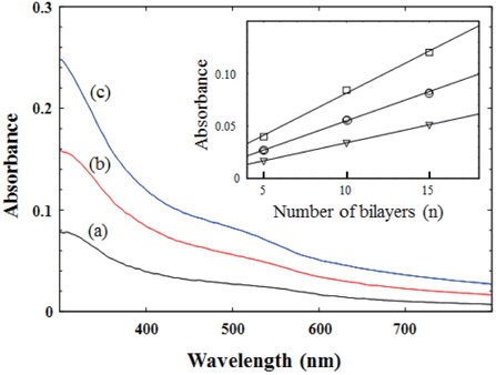
Figure 1 shows the UV/Vis absorption spectra of self-assembled (CdTe/PSS)n films on glass substrates, where n = 5, 10 and 15. A weak shoulder was observed near ~500 nm in each spectrum, which was originated from the surface plasmon of CdTe nanoparticles firmly bound to the PSS in the multilayered films. PSS itself has a very negligible contribution to the absorption spectra. Absorbance of the films increased in accordance with the increasing number of bilayers. Absorbance of each spectrum at 400, 500 and 600 nm was plotted on the number of bilayers (n), as shown in the inset of Figure 1. A linear proportion of absorbance to the number of bilayers denotes that an equal amount of CdTe was adsorbed after each dipping cycle [2-4]. This result suggests that the polyanion (PSS) is effective to adsorb cationic CdTe in the next layer [2].
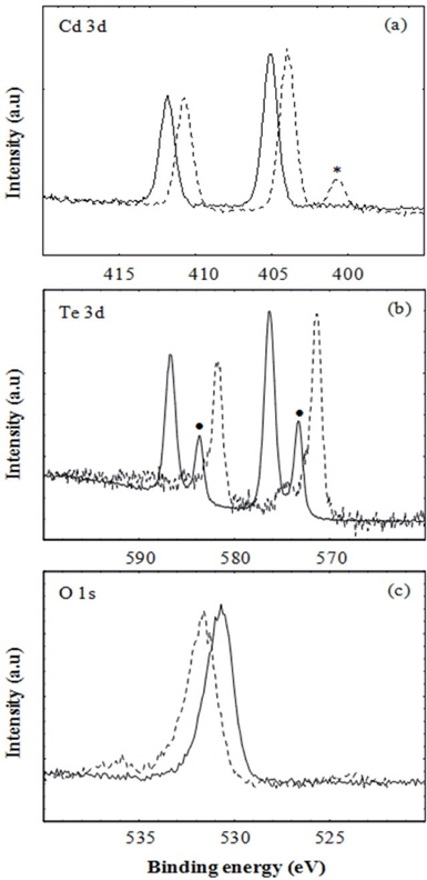
XPS data are important evidence to analyze the stoichiometry and binding characteristics of each element in a given composite system in terms of its energy change [22-24]. Depending on the contact environment, the resulting binding energies of a given element can be shifted towards the higher or the lower position [22-26]. Binding energy changes in the XPS measurement are caused by the redistribution of interfacial electron cloud due to the strong interaction between the neighboring elements [22,25,26]. Figure 2 shows the XPS results obtained from CdTe nanoparticles, PSS and their (CdTe/PSS)15 film. The binding energies of CdTe in this film were compared with those of CdTe nanoparticles alone in Fig. 2(a) and (b). It was found from the XPS data, that the binding energies of Cd and Te in (CdTe/PSS)15 film shifted towards the higher energies; (Cd 3d3/2 and 3d5/2) 410.7 eV and 404.0 eV for CdTe nanoparticles, and 411.8 eV and 405.1 eV for CdTe/PSS composite film, (Te 3d3/2 and 3d5/2) 581.7 eV and 571.4 eV for CdTe nanoparticles, and 586.7 eV and 576.3 eV for CdTe/PSS composite film. These higher shifts might be caused by the strong attraction between the counter-charged PSS and CdTe [8]. The strong attractive interaction could stabilize the nanoparticles bound to the PSS, thereby resulting the surface electrons of CdTe nanoparticles to shift towards the higher binding energies [22]. Binding energy shifts of Cd and Te in (CdTe/ PSS)15 film were much higher than those of Cd and Te in the c- MWNT-CdTe composite. CdTe nanoparticles were bound to the sidewalls of carboxylated MWNTs (c-MWNTs) in the c-MWNTCdTe composites [22]. This higher shift of binding energies could be explained by the alternate adsorption of PSS and CdTe; the counter-charged PSS or CdTe were sequentially and completely surrounded by the others (CdTe or PSS). Therefore, the surface electrons of CdTe nanoparticles could be significantly influenced by the more electronegative oxygen atom of the PSS molecules. The binding energies of the O atom in CdTe/PSS film and pure PSS were compared in Fig. 2(c). O1s peak of (CdTe/PSS)15 film, which was originated from PSS, shifted towards the lower binding energy than that of the PSS alone; 531.6 eV for PSS alone and 530.7 eV for (CdTe/PSS)15 film. The lower shift of the binding energy was engendered by the strengthening of the electrical contact [26-28]. It has also been reported in our previous work, that the binding energies of some elements in an oppositely-charged composite system can shift towards the lower or the higher position depending on the characteristics of the composite system [29]. The changes of binding energies indicate that oppositelycharged PSS and CdTe were bound well by the electrostatic interaction.
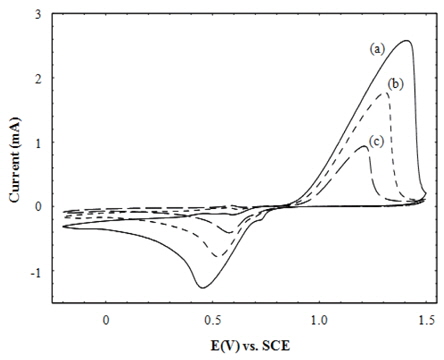
Cyclic voltammetry (CV) is one of the useful techniques for achieving the electrochemical information of a given sample as well as to analyze the qualitative information and mechanism of redox (reduction and oxidation) reactions by monitoring the current, intensity and position of the peak potential on the applied voltage [23,29,30]. The electrochemical behavior of the multilayered CdTe/PSS films was studied elaborately by CV in this work. Figure 3 shows the cyclic voltammograms of Au electrode, PSS/ PEI and (CdTe/PSS)1 films. They were oxidized and reduced at the applied voltage ranging from 1.31 to 1.11 V, and from 0.52 to 0.68 V, respectively. Although a trace and negligible oxidation and reduction were observed in the ranges of 0.53 to 0.63 V and -0.17 to 0.11 V, respectively, it is considered that these tiny redox peaks scarcely contribute to the electrochemical behaviors of the multilayered films. Their current intensities on redox reactions decreased in the order of Au, PSS/PEI and (CdTe/PSS)1. Moreover, the peak positions shifted towards zero potential with the same order. In the CV experiment, redox reactions begin from the materials close to the electrode surface under a periodic change of potential, and the corresponding electronic transfer occurs between the materials close to the electrode and the electrolyte, thereby resulting in cyclic currents. This figure evidently shows that the alternate deposition of PSS and CdTe changed the redox peak positions and their cyclic currents. When an additional component is deposited on the analyte close to the working electrode, it can enhance or restrict the electron transport and influence the cyclic current intensity [23]. Figure 3 shows that the alternate depositions of PSS and CdTe considerably reduced the redox current of the electrodes. In addition, the shift of peak potential indicates that the electronic energy status of the deposited material was changed with the sequential depositions on the electrode, which agree with the XPS results [23,29,31].
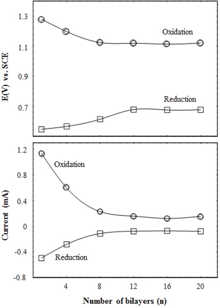
To study the changes of cyclic current intensity and peak potential with the voltage applied to the working electrode in terms of film thickness, the current intensities and the potentials of redox peaks were measured; they were then plotted against the bilayer numbers of multilayered CdTe/PSS film, as shown in Fig. 4. With the increase of bilayers up to 8, the oxidation and the reduction peaks shifted towards the lower and the higher potentials, respectively. Their cyclic current intensities changed towards the zero value in both oxidation and reduction; (oxidation) 1.13 to 0.23 mA, (reduction) -0.5 to -0.11 mA. The decline in the current intensities implies that the electrons become gradually hard to transfer in the medium. Correspondingly, this could be caused by the increase of contact interfaces between the CdTe/PSS bilayers. The current intensity decrease continued up to 8 bilayers of CdTe/PSS and kept at the bottom level for over 8 bilayers. Meanwhile, the change of the characteristic redox potentials indicates that the HOMO and the LUMO energies as well as the band gaps were changed by the formation of CdTe/PSS composite films. Such evidence could be found in our previous work [29]. As aforementioned, these potentials were changed by the iterated deposition of the CdTe/PSS bilayer. HOMO/LUMO energy levels could be estimated through analyzing the oxidation and reduction potentials obtained from the CV results [29,32- 34]. The decrease in the oxidation potential causes the rise of the HOMO energy level. On the contrary, the increase of the reduction potential implies the decline of the LUMO energy level. These energy levels preserved over 8 bilayers of CdTe/PSS films. Adjustment of the energy band gap can be an important factor for determining the efficiency of device, such as solar cell, which is composed of multilayered structures. In particular, this result can be usefully applied to the solar cell system based on CdTe nanoparticles. The energy levels of the adjacent layers should be carefully adjusted in order to separate the electron-hole pairs effectively. Considering the Shockley-Queisser limit, the energy band gap should be suitably tuned in order to apply for the solar cell system [35].
Multilayered CdTe/PSS films were prepared by an electrostatic self-assembly method in an aqueous medium. The linear relationship of absorbance and the number of CdTe/PSS bilayer indicates that the repeated depositions of CdTe and PSS were properly built up on a glass substrate. The binding energies of elements were shifted upwards or downwards according to the attractive interaction in multilayered CdTe/PSS films; the binding energies of Cd 3d and Te 3d moved upwards and that of O1s moved downwards. It is found that the multilayered CdTe/PSS films, which were prepared by the iterated depositions of CdTe and PSS, made the homogeneous composites through the entire thickness. Cyclic currents and potentials in cyclic voltammograms were gradually changed with the increase of CdTe/PSS bilayers, which are closely related to the variation of HOMO and LUMO energy levels of the multilayered films. These currents and potentials kept the similar values for over 8 bilayers.