Recently hydrogenated amorphous silicon (a-Si:H) waveguides have attracted significant interest for their potential applications to nonlinear optic devices because the a-Si:H material has a relatively high-nonlinear-optic property compared to the crystalline silicon, and can be easily obtained for device fabrication with the complementary metal-oxidesemiconductor (CMOS) device process [1-3]. While the conventional silicon waveguides are formed on the silicon-oninsulator (SOI) wafers which are produced through a delicate wafer-bonding process, the a-Si:H waveguides can be formed on an a-Si:H layer which is deposited directly on the conventional silicon wafer with using a plasma-enhanced chemical vapor deposition (PECVD) process after a silicondioxide (SiO2) bottom layer deposition. Furthermore, the amorphous silicon can be formed in the multi-stacked layers, thus offering much freedom for complex device fabrication. Recent technological development has shown a significant reduction of the optical loss which is comparable to that of the single-crystal silicon. In addition, the a-Si:H waveguides have been used for photon pair generation through the fourwave- mixing (FWM) process [4, 5].
Nonlinear optic devices, especially correlated photon-pair generation devices based on the FWM process, require not only low optical-loss of the a-Si:H material but also the optimized chromatic-dispersion (CD) property of the waveguides [2, 6]. The CD property affects the phase-matching condition among the pump, signal and idler beams in the FWM process, and thus influences the efficiency of the FWM-beam generation. The CD properties of nano-scale waveguides have been analyzed extensively for the crystalline silicon [7-12], and it has been known that their CD properties depend significantly on waveguide size even for the same core and clad material structure. The core-dimension-dependent CD properties and nonlinear effect of the crystalline silicon waveguides have been investigated in the previous reports. However, no detailed analysis on the CD properties and nonlinear effect of the a-Si:H waveguides has been reported yet.
In this paper we report on the experimentally measured CD properties of the a-Si:H waveguides of 220-nm thickness having three different widths of 400, 450 and 500 nm, and on their comparison with numerically simulated results. We also present their effect on the FWM-signal-generation efficiency based on experimentally measured and numerically calculated results.
II. WAVEGUIDE DESIGN AND FABRICATION
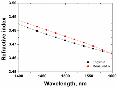
The spectral profile of the refractive index of the a-Si:H material was measured with an ellipsometer after a thin film deposition with the PECVD process on the top of a SiO2 layer which was also formed directly on a silicon wafer. The a-Si:H film was deposited at a gas-mixing condition of 1:15 ratio of a precursor gas Silane (SiH4) and a hydrogen gas (H2), at the total gas pressure of 2.0 torr, at an RF power of 100 W, and at a substrate temperature of 300℃. Figure 1 shows a refractive-index profile of the a-Si:H layer measured by using the ellipsometric method and compared with the known refractive-index values of the a-Si:H material [13]. The measured refractive index of the a-Si:H layer at the He-Ne laser wavelength of 632.8 nm was 4.0423. By comparing this value with the data reported by R.J. Severens
Three types of the a-Si:H waveguide with a fixed height of 220 nm but with three different widths of 400, 450 and 500 nm were designed and fabricated. Before fabrication of the a-Si:H waveguides, the SiO2 layer was first deposited into a 2-μm thickness at a temperature of 400℃ on a 750- μm-thick silicon wafer as a bottom-cladding layer using the PECVD process. Then, a chemical-mechanical-polishing (CMP) process was performed to achieve a smooth top surface of the SiO2 layer up to the root-mean-square (RMS) surface roughness of about 0.4 nm as it was measured by an atomic-force microscope (AFM) within a 5-μm×5-μm area. In the next step, a 220-nm-thick a-Si:H layer was deposited on the SiO2 film by using the PECVD method. Electron-beam-lithography and dry-etching processes were then applied to fabricate waveguide patterns on the a-Si:H layer. The fabricated a-Si:H waveguides had the same 220-nm height but three different widths of 400, 450 and 500 nm. The waveguides had 200-μm-long inverse-taperedcoupling sections at both ends with a 100-nm-wide-end cross section. The a-Si:H layer was covered with a SiO2-layer upper cladding. Integrated Mach-Zehnder-interferometer (MZI) devices with two arms of asymmetric lengths were also fabricated with each of the three different-thickness waveguides for measurement of each group index.
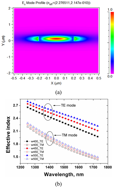
The effective refractive indices of the waveguides for light-beam propagation of transverse-electric (TE) and transverse-magnetic (TM) modes were calculated by using a commercial software based on the finite-element method (Rsoft FEMSIM), and were used for calculation of the CD values. The calculated TE-mode profile in the a-Si:H waveguide of a 220-nm×450-nm cross-section embedded in the SiO2 material is shown in Fig. 2(a). The calculated effective-index profiles of the three different waveguide widths are plotted in Fig. 2(b). In this calculation, the Sellmeier equation of the silica (SiO2) material [15] and the measured refractive-index profile of the PECVD-deposited amorphous silicon were used. The calculated effective indices of the TE mode are larger than those of the TM modes. Based on these effective-index values of the waveguides, the group indices and CD values were obtained, and compared with the measured results, as discussed in the next section.
3.1. Group Index Measurement and Chromatic Dispersion Determination
The group-index (GI) profiles of the fabricated a-Si:H waveguides were determined by measuring the interferencespectrum output of the MZIs under illumination of an amplified super-luminescent diode (SLD) at the 1.5-μm -wavelength range with an erbium-doped-fiber amplifier (EDFA). The polarization of the amplified-SLD output was adjusted with a polarization controller (PC), and selected to either one of the waveguide TE and TM modes with a fiber-type polarization-beam-splitter (PBS) of a 30-dB extinction ratio. The light was launched into and collected from the inversely tapered ends of the a-Si:H waveguide by using tapered polarization-maintaining-fibers (PMFs) at both ends. The transmitted output beam of the MZIs was measured by an optical spectrum analyzer (OSA) with a 70-pm resolution.
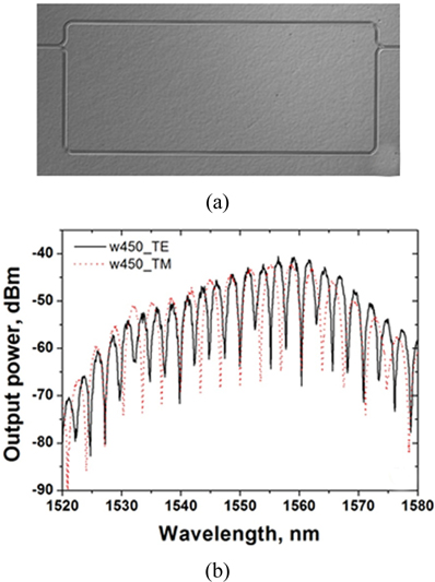
Figure 3(a) shows an optical microscope image of the fabricated MZI with the 220-nm×450-nm a-Si:H waveguide. The MZI was formed with two Y-branches and with a path-length-difference of 200 μm between two arms. The bending radius of the Y-branches was about 5 μm. It is known that, as long as the bending radius was larger than 2 μm, optical loss at the bending region was negligible, and waveguide-dispersion impact was minimal. From the path-length difference between two arms, a relative phaseshift occurred between two light outputs passing through the arms. As a result, the interference fringes at the output of the MZI were measured. The measured spectralinterference output of the MZI is shown in Fig 3(b). Measured extinction ratios of the MZI-interference spectra were about 20 dB and 25 dB for TE and TM modes, respectively. Since the relative phase-difference between a peak and its adjacent minimum valley was equal to
where λ
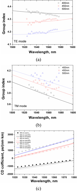
Figures 4 (a) and (b) show the measured group-index profiles of the a-Si:H waveguides for the TE and TM modes, respectively, obtained from the measured interference fringes. Each plot with a different symbol represents the measured group-index values for each of the waveguides of three different widths. The line curves indicate the calculated group-indices based on the spectral effectiveindex profiles shown in Fig. 2(b). The group index can be calculated from the effective refractive-indices using the following relationship [14].
The plots indicate that the measured group index
where
The CD values of the waveguides was measured experimentally by using a white-light interferometer (WLI) method [11] and also determined from the measured group index profiles. Spectral profile of the phase changes in the interference spectra of the WLI outputs was measured when a reference sample placed in one arm of the WLI was replaced with an a-Si:H-waveguide sample, and used to determine the precision CD values of the sample. The obtained CD coefficients of the a-Si:H waveguides of three different widths are plotted in Fig. 4(c) with symbols indicating the data obtained from the measured group index values, with solid lines corresponding to the experimental results measured using the WLI method, and with dotted lines representing numerical results calculated from the
3.2. Four-wave-mixing Process in a-Si:H Waveguides
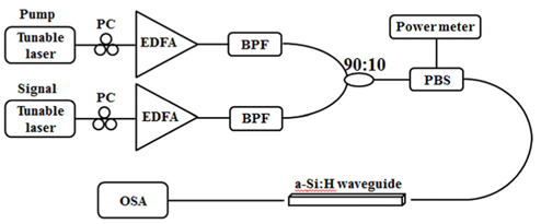
The experimental setup used for the FWM measurement is illustrated in Fig. 5. Two tunable lasers were used as pump and signal beam sources for the FWM experiment with the a-Si:H waveguides. The pump wavelength was fixed at 1532 nm while the signal wavelength was swept from 1520 to 1570 nm. The tunable-laser-source signals were amplified with high-power erbium-doped-fiber amplifiers (EDFAs). After amplification through the high-power EDFAs, the ASE noises from the amplified pump- and signalbeams were filtered out with narrow band-pass filters. The polarizations of the pump- and signal-lightwaves were aligned to the same TE-polarization direction of the waveguide with PCs and a fiber-type PBS. Then, the two lightwaves were combined with a 90:10 coupler, and their TE-polarization beams were inputted into the a-Si:H waveguide in its TE-mode direction via the PBC and a tapered PM fiber. The optical output from the a-Si:H waveguide was measured with an optical spectrum analyzer (OSA). Three different a-Si:H waveguides with cross-section sizes of 220-nm height and of 400-nm, 450-nm and 500-nm widths but all with the same waveguide length of 6 mm were used for the FWM-signal-conversion-efficiency measurement. Propagation losses of the three waveguides were about 0.67, 0.55 and 0.45 dB/mm, respectively, for the TE-mode. Our a-Si:H waveguides had higher propagation losses than others reported in Refs. 4 and 5. This might be attributed to non-optimized sidewall roughness of our waveguides. The fiber coupling loss to the inverse tapered waveguide end was about 11 dB/facet for the TE-mode beam input.
The signal-idler generation efficiency through the degenerated FWM process can be analyzed with the coupled-mode equations [18, 19]:
where
where
If we expand the wave propagation constant using Taylor series about a reference frequency (i.e. a reference wavelength)
From Eqs. (3), (8) and (9), the linear phase-mismatch
where [
The FWM-signal-conversion efficiency is defined as
where
The FWM-signal-conversion efficiency was calculated with an assumption that the coupling losses of the signal beam both at the output and input coupling sections were the same and the idler beam had the same coupling loss at the output coupling section. The coupling loss and waveguide loss were determined by using the same-type a-Si:H waveguides of various lengths as described in Ref. 11. Then, the input signal power
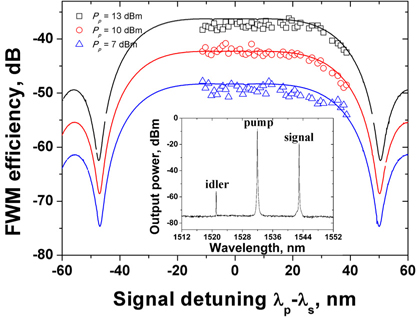
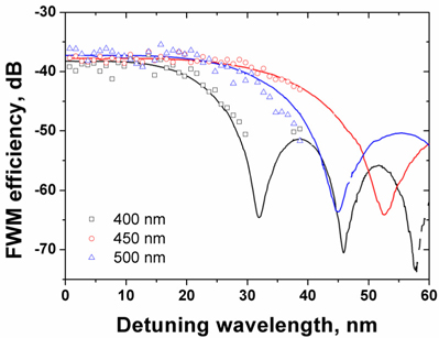
The measured FWM-signal-conversion efficiencies of the 400-, 450- and 500-nm-wide a-Si:H waveguides with a fixed pump-beam of 1532-nm wavelength are shown in Fig. 6 with marks of open squares, circles, and triangles, respectively, and compared with the calculated ones from the coupled-mode equations in Eqs. (4) to (7). As shown in Fig. 4(c), the two waveguides of 450-nm and 500-nm widths have the anomalous GVD at wavelengths around 1530 nm, and have wider wavelength ranges for an efficient FWM process than the 400-nm-wide waveguide does. For these measurements, the coupled pump-power was fixed to +13 dBm.
The wavelength range of the 3-dB-drop FWM-beam generation efficiency from the peak value covers about 42, 75 and 65 nm for the 400-, 450- and 500-nm-wide waveguides, respectively. Since the zero-dispersion wavelength of the 220-nm×450-nm waveguide is close to the pump wavelength of 1532 nm, the signal light can be tuned in a wide wavelength-range for relatively high FWM-beam-generation efficiencies compared to the other size waveguides. It is expected that the FWM-beam-generation bandwidth will be extended over 100 nm if the pump wavelength is tuned close to the zero-dispersion wavelength.
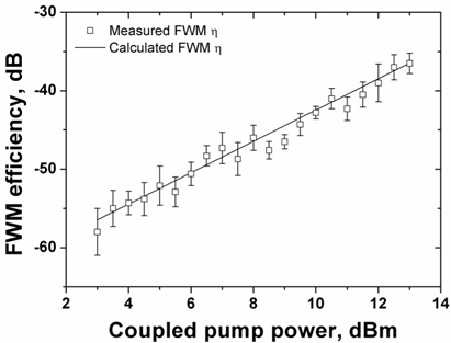
The measured FWM-beam-generation efficiencies for various coupled-pump-powers at 1532 nm in the TE-polarization- mode of the 220-nm×450-nm waveguide are plotted with symbolic marks in Fig. 7. The calculated FWM efficiencies are also plotted in the same figure. The FWM efficiency was -35 dB at the coupled pump-power of +13 dBm, and decreased as the coupled pump power was reduced. The full wavelength range for the efficient FWM-beam-generation could not be measured experimentally due to the limited-wavelength coverage of our experimental equipments. The inset in Fig. 7 shows the measured FWM spectrum with the 1532-nm-pump and 1543-nm-signal beam wavelengths.
The nonlinear refractive index of the a-Si:H material was determined by varying the
Figure 8 shows the measured and the calculated FWM-beam-generation efficiencies of the 220-nm x 450-nm waveguide as a function of the coupled pump-power at 1532-nm wavelength. In the logarithmic scale of both xand y-axes, the FWM efficiency is almost linear with the pump power in a range from +3 to +13 dBm. The FWM-efficiencies calculated numerically by using Eqs. (4) to (7) match well with the measured results within the experimental error bars, which correspond to the standard deviations from the mean values of five measurement runs at each coupled pump-power. Our measured FWM conversion efficiencies are a little lower than those reported in Ref. 1 probably due to a relatively high waveguide loss of our sample compared to the other’s. A further improvement can be made by having a uniform material property of the a-Si:H layer and smooth surfaces via a fine vertical-side wall etching.
In this paper, we have presented experimentally-measured and numerically-calculated results of the chromatic-dispersiondependent FWM-beam-generation efficiencies of three different a-Si:H waveguides of 400-, 450- and 500-nm widths but of a fixed 220-nm height. The effective group indices of the three different a-Si:H waveguides were determined by fabricating integrated Mach-Zehnder interferometer (MZI) devices of asymmetric arm lengths with the a-Si:H waveguides and by measuring their interferencespectrum outputs, and compared with the numerically calculated values from the effective refractive indices of the waveguides which were obtained with the Sellmeier equation for the SiO2-clad material and with the measured refractive-index profile of the a-Si:H core. Then, from the spectral profiles of the effective group indices, the CD values of the waveguides were calculated, and compared with experimentally measured CD values using a whitelight interferometric method.
The three different waveguides, all with 6-mm-long length and with tapered ends on both sides, were also used for measurement of the FWM-beam-generation efficiency with a fixed pump-wavelength of 1532 nm but with varying the signal-wavelength in the range from 1520 to 1570 nm. Among the three different waveguides of 400-, 450- and 500-nm widths, the FWM efficiency and the wavelength range of the efficient FWM conversion were the maximum for the 220-nm×450-nm a-Si:H waveguide because its zero CD wavelength was close to the pump wavelength.
Based on these results we could conclude that the CD profile of the amorphous silicon waveguide plays a critical role to the wide wavelength-range for an efficient FWM process compared to the pump power. The maximum FWM-efficiency of the waveguide was -35 dB for the coupled pump-power of +13 dBm, and the FWM-conversion wavelength-range was about 75 nm. Our devices used in this research were not optimized for low coupling and insertion losses. Further improvement on the FWM-efficiency in a-Si:H waveguides could be possible by having a low-loss characteristics of the waveguides through optimization of the device fabrication processes.

![Measured refractive-index profile of the a-Si:H film compared with the known values [13].](http://oak.go.kr/repository/journal/13813/E1OSAB_2013_v17n5_433_f001.jpg)