A digital micromirror device (DMD) is a spatial light modulator, which consists of hundreds of thousands of micro-scale mirror pixels. Each pixel is independently controllable and bi-stable [1]. A DMD has the advantages of high contrast ratio and throughput and a wide dynamic control range [2]. Because of this, DMDs have been widely used in various applications such as projectors [3,4], confocal microscopes [5-7], and maskless lithography [8-14].
Maskless lithography has attracted a great deal of attention because it circumvents the high costs of conventional photolithography, namely the fabricating and maintaining of photomasks. Various maskless lithography techniques have been developed, such as plasmonic lithography [15], zone plate array lithography (ZPAL) [16, 17], and nanoimprint lithography [18]. Among the various maskless lithography techniques, researchers have developed ML systems based on DMDs and subsequent applications since Chan et al had proposed a DMD-based ML system [8, 9]. The DMD-based ML system has high throughput for highly customized patterns and is cost- and time-efficient.
In an ML system, the DMD serves the same role as the photomask in conventional photolithography. Each DMD mirror pixel can be assigned a value—either 0 (“off”) or 1 (“on”). The pixel rotates +/- 12° to its assigned value along a diagonal line. The direction of the pixel’s reflected beam can be controlled either into or outside of the exposure system by its rotation state. DMD defects—also referred to as “DMD malfunctions”—obstruct the intended pattern transfer and cause a decrease in pattern quality. In particular, there is a chance that any type of malfunction will arise in DMDs as a result of operation at the extremes of its capabilities. For example, high throughput generally requires that the light source have greater power than conventional applications—such as projectors—as well as be capable of continuous maximum speed DMD operation. As a result, it is necessary to inspect DMDs regularly to ensure perfect mask image transfer.
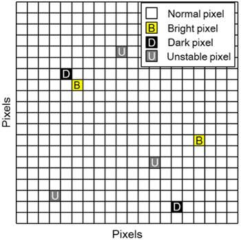
Several methods for detecting bright and dark DMD pixels have been suggested previously [19, 20]. Bright, dark, and unstable pixels are all representative types of bad DMD pixels [21]. However, these methods are not applicable to ML DMD inspection because unstable pixels [21] and input and output frame data cannot be inspected readily. We divide DMD malfunctions into two general types: mechanical defects and data transfer errors. In mechanical defect inspection, unstable pixels are examined simultaneously with bright and dark pixels. Because of the need for high throughput in the ML field, high speed DMD operation is required; each frame’s data transfer state must be checked under high-speed DMD operation. Essentially, data transfer errors which represent mismatch of the input frame and output frame is also considered. In the present work, we propose two methodologies to detect mechanical defects and the data transfer errors. We also develop an optical inspection system and evaluate DMD malfunctions under their maximum speed operation setting, 28000 frames per second (fps).
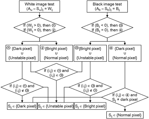
Bad pixels are detected by comparing the input and output image frames to each other. The image frames can be regarded as 2-dimensional matrices with the same size as the DMD array itself. The image frame output is the optical image of the DMD formed on a CCD by a projection lens and can be reflected by the actual state of each micromirror of the DMD. Both image frames are matched geometrically, so each mirror pixel can be evaluated by comparing the two image frames. To classify the type of pixels into normal, bright, dark and unstable pixels, we used just 2 images (a white and a black image), a simple and time effective method. The white image is composed of only ‘on’ pixels whereas the black image is composed of only ‘off’ pixels. A bright pixel appears as a white dot when other micromirrors are turned off; similarly, a dark pixel appears as a black dot when other pixels are turned on [21]. As a result, bright and dark pixels can be detected by image tests of the opposite state [21]. Unstable pixels show random motion regardless of the input data and appear as a gray dot in both tests [21]. We typically require multiple identical images of each image test to identify unstable pixels.
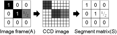
We define the image frame as a matrix A and the segment matrix S to be the resulting matrix that is converted from the optical image of the DMD into a 2-dimensional matrix that is the same size as A. S shows the actual state of each micromirror (Fig. 1).
In the matrix, 1 stands for “on” state pixels, 0 for off state pixels and a random value between 0 and 1 for unstable pixels S. The bad pixel classification algorithm is depicted in Fig. 2.
In the white image test, bright and normal pixels in A and S all have the same value (“1”) at the same time, whereas dark pixels and unstable pixels have a value less than 1. As a result, the set of dark and unstable pixels (numbered ① in Fig. 2) is distinguished from the set of bright pixels and normal pixels (②) by comparing A and S. In the black image test, the set of bright pixels and unstable pixels (③) is similarly easily distinguished from the dark and normal pixels (④). The location of unstable pixels is obtained by finding the intersecting set of locations between the 2 sets (①, ③). Accordingly, the location of dark pixels and bright pixels can be obtained by finding the difference set of (①, ③) and (③, ①), respectively. Finally, the location of normal pixels can be obtained by finding the difference set between the set of dark and normal pixels (④) and the set of dark pixels.
2.2. Data Transfer Errors Detection
To detect data transfer errors, the agreement of the input frame data with the corresponding output frame data must be verified at each pixel. Because there is no relation between data transfer error and the value of the input frame data, any input image frame can be chosen to detect data transfer errors. The direction of the reflected beam at a pixel can be controlled by the data transferred to the pixel. We chose input image frames consisting of repetitive “on” and “off” states so that the optical signal of the reflected beam has a frequency. We compared the frequency of the input frames to that of the output optical signal. The expected frequency of the output optical signal is half of the input frames’ frequency. The relationship between the two signal frequencies is described as:
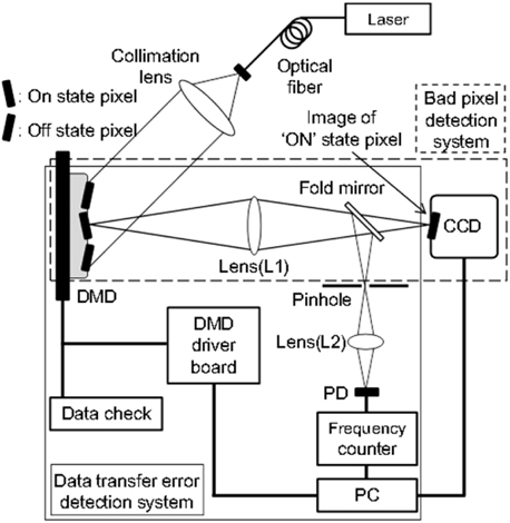
The layout of the optical inspection system used in this work to detect DMD malfunctions is depicted in Fig. 3.
The system has 2 functions. The upper part contained within the dashed line is used to image DMD pixels to detect bad pixels and the lower part bounded by the solid line is used to detect data transfer errors.
The optical source is a 532 nm laser with 100 mW of power. The laser beam is routed to the collimation lens with an optical fiber. We then used a neutral density filter to reduce the power to preventing CCD signal saturation. The beam diameter is expanded to 5 mm, which covers an area of approximately 200×200 DMD pixels. The intensity difference among 20×20 DMD pixels is corrected by image processing by assuming that the intensity distribution of the beam is Gaussian. The incident angle of the collimation beam on the DMD surface is twice the DMD tilt angle, so that the beams from “on” micromirrors are reflected to the direction normal to the DMD window. We used a DMD (DiscoveryTM 4100, Texas Instruments) with 1024×768 pixels. The pixel pitch is 13.68 μm and the maximum frame rate is 28000 fps. The tilt angle of this model is ±12° and a driver board (LibertronTM) forms the DMD interface. Image frames generated in the driver board are transferred to the DMD. The DMD loads the image frames from memory and all mirrors change their state simultaneously after receiving a reset command.
Only beams from “on” mirrors are transferred through the aperture of the lens L1. The CCD camera is a 1/3 inch progressive scanning type with a 1024×768 square pixel array, a 10 bit depth, a 4.65 μm pixel pitch, and a signal to noise ratio of greater than 10. We set the magnification to 5.8 for easier recognition of the micromirror image. In this situation, a single micromirror is imaged on approximately 17×17 CCD pixels. The f-number of the lens L1 is limited to accept only the “on” state DMD beam; they must therefore be larger than f/2.4. In this experiment, we were required only to resolve the micromirrors. The minimum resolution required for this system to recognize each individual micromirror is 6.8 lp/mm on the image plane of lens L1; the f-number must thus be smaller than f/30 to achieve the necessary resolution. We selected an achromatic doublet lens (AC254-100-A1, Thorlabs) as the projection lens (L1). The full aperture size of the lens L1 is 25 mm, and we set the aperture size to 15 mm to set the f-number of the projection lens to 6.7 by placing a mechanical aperture. In this configuration, the MTF is 0.5 at 17 lp/mm, close to the diffraction-limited performance regime. The MTF value at the required spatial frequency is acceptable for normal CCD imaging. Therefore, the selected lens (L1) is sufficient for our purposes. Each CCD image is gathered by a frame grabber into the PC, which converts the CCD images into segment matrices and bad pixel maps by comparing image frames and segment matrices according to the bad pixel classification algorithm.
In addition, a lens (L2), a pinhole, a photodiode and a frequency counter are set up to measure the reflected beam from a particular pixel, referred to as the target pixel. By applying the fold mirror, only the beams reflected by the “on” state of the target pixel are transferred through the pinhole, which is then received by the lens (L2) and the photodiode (S1337-33BQ, HAMAMATSU). The optical signal received at the photodiode is converted to an electric signal. The rise time of the photodiode is 0.2 μs, much shorter than the 35.7 μs period of the DMD at its maximum frame rate (28000 fps). The photodiode is thus more than sufficient for recognition of each frame of DMD operation. The frequency counter (AFG-2105, GW Instek) measures the frequency of the electric signal. The frequency counter can cover a measurement range of up to ~150 MHz, much higher than the maximum DMD frame rate, and has a measurement accuracy of ±1 fps.
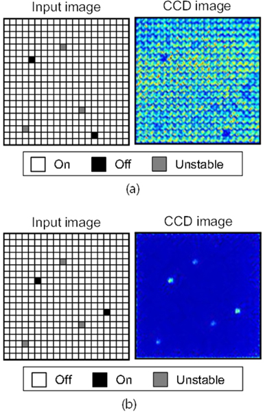
To verify the efficacy of our bad pixel detection algorithm, we performed a test using a 20×20 pixel DMD array. In the black and white image tests, two image files are generated as input image frames. We included two each of bright, dark, and unstable pixels at various positions in the input image frames as a test. The real pixel states in the black and white image tests and their results are depicted in Fig. 4.
After loading the two image frames into the DMD driver memory, the DMD starts each image test. The CCD camera captures each moment of the test. This process yields two CCD images. The bad pixel detection algorithm is then run, comparing the input image frames with the segment matrices.
In the white input image, two “off” state pixels, 3 unstable state pixels and the rest “on” state pixels operate. Unstable pixels switch randomly between the “on” and “off” states. In the black input image, two “on” state pixels, 3 unstable pixels and the rest of the “off” state pixels operate. The unstable pixel locations are the same in both input images.
The locations of the dark and unstable pixels are obtained from the white image test result, while those of the bright and unstable pixels are obtained in the black image test. The bad pixel map was then built by the bad pixel classification algorithm.
As shown in Fig. 5, we obtained a map that clearly identified each of the bad pixel types—bright, dark, and unstable pixels. All bad pixel locations were identified correctly at the included locations and the remainder were identified as normal pixels.
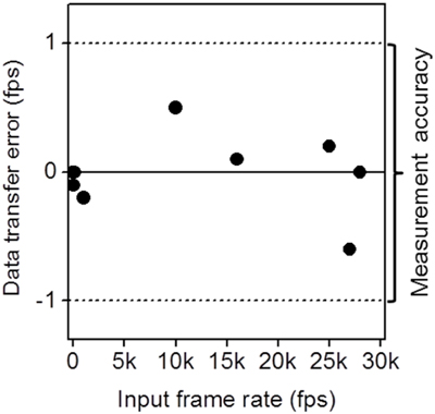
To detect data transfer errors, input image frames with repetitive “on” and “off” states (1 frame) at a target pixel are chosen. The experiment is conducted at different DMD frame rates between 1 and 28000 fps (1, 10, 100, 1000, 10000, 16000, 25000, 27000, 28000 fps). The test results are shown in Fig. 6. Each point represents the difference between the reference frequency and twice the measured frequency at a given DMD frame rate. We found that all frame rate errors are below the measurement accuracy (±1 fps) of the frequency counter in all frame rate scenarios, implying that no data transfer errors occurred between the DMD driver board and the DMD itself. The input frame data and operation of the target pixel are thus in good agreement.
In this study, we suggested two methodologies for detection of DMD malfunctions. One detection algorithm classifies bad DMD pixels and the other detects data transfer errors. We designed a DMD inspection system that can replace current mask inspection methods for DMD-based DML. To verify the feasibility of our system we performed two tests.
For detection of bad pixels, we successfully classified bright, dark, and unstable pixels and detected their locations. The method uses a white and a black image and reduces the amount of testing time required; it is expected that the time savings would be greater for high pixel density DMDs. Whereas the time required to test with the single pixel scanning method depends on the DMD array size—a total inspection time of M×N×T for a M×N DMD micromirror array when T is the testing time for a single pixel—the inspection time for our method is independent of DMD array size, 2×T. For a DMD with a 1024×768 micromirror array, our bad pixel detection method is about 390,000 times faster than the single pixel scanning method.
For our data transfer error detection method, we verified that there are no data transfer errors in the test by confirming the agreement between the input frame rate and the output frame rate within the measurement accuracy (1 fps).
Our system provides easy methods to identify DMD malfunctions in DML systems and can be applied to evaluate the operation quality of DMDs in any field in which DMDs are adopted.