검색 전체 메뉴
PDF
맨 위로
OA 학술지
Design of Metamaterial-Inspired Wideband Absorber at X-Band Adopting Trumpet Structures
  • 비영리 CC BY-NC
  • 비영리 CC BY-NC
ABSTRACT
Design of Metamaterial-Inspired Wideband Absorber at X-Band Adopting Trumpet Structures
KEYWORD
Absorber , Metamaterial , Trumpet Structure , Wideband , X Band.
  • I. INTRODUCTION

    Electronic warfare has become an important issue in the current military environment. Suppression of unwanted scattering from conducting bodies is especially critical; consequently, much research is presently focused on low radar cross sections (RCS) using absorbing panels. Conventional ferrite tile absorbers are effective (typically about 20 dB absorption) in the frequency range below 1 GHz, but these are ineffective near the X-band.

    Recent advancements in metamaterial research have opened the possibility for the development of a metamaterial absorber (MA) through microstructure engineered materials. The goal of a MA is to completely absorb the electromagnetic waves over a particular frequency band. The most common designs have been based on split-ring type resonators (SRRs), which have been widely studied for negative permeability and double negative metamaterial [13].

    However, SRRs have an inherent preferred polarization direction and exhibit poor performance characteristics at oblique incidence angles. They also typically suffer from narrow bandwidth due to the highly dispersive nature of the structures. Many other designs have been suggested to improve the bandwidth of the absorbers, such as the Minkowski fractal frequency selective surface and two-layer structure [4,5]; however, these attempts further complicate the structure. A resistive pattern with a pre-defined surface resistance has also been studied for large-scale production and cost reduction [6].

    In this letter, we present two types of metamaterial-inspired absorbers that adopt resistive trumpet structures. The proposed absorber exhibits nearly complete absorption over a wide frequency band (X-band) if well optimized, due to the inherent wideband nature of the trumpet structure that is used. It is also almost polarization-insensitive owing to the proposed symmetry.

    II. DESIGN AND SIMULATION RESULTS OF PROPOSED ABSORBERS

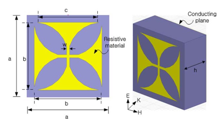
    Fig. 1 shows the geometry of the proposed absorber (case 1). The optimized geometrical dimensions of the proposed unit cell are: a = 5.6 mm, b = 4.6 mm, c = 4.2 mm, w = 0.2 mm, s = 0.3 mm, g = 0.5 mm, h = 2.4 mm. The crossed trumpet-shaped surface structure and the metallic back plane are made of copper. The substrate is FR-4 with a permittivity of εr = 4.4–j 0.02. When an electromagnetic wave is normally incident on the trumpet structure, its impedance resembles that of a series RLC resonator. If it is placed roughly one quarter wavelength against a conducting plane, the total input impedance becomes that of a parallel connection of the trumpet structure (similar to a series RLC resonator) and the shorted λ /4 transmission line resonator (similar to a parallel LC resonator). When the overall dimensions, together with the chip resistor value, are well optimized to have an input resistance close to 377 Ω (that of free space) and input reactance close to 0 Ω over a wide frequency band, the design is complete. This has proved possible, particularly due to the reactance (or susceptance) cancelling effect of the used two resonators. These absorber dimensions, together with the 65 Ω lumped resistors, give optimized results for high absorption and maximized bandwidth. The proposed absorber has been designed assuming a metallic back plane, which could represent, for instance, the surface of an aircraft. The first design using chip resistors can be replaced by similar surface patterns having uniform surface resistance per square, which will be addressed later.

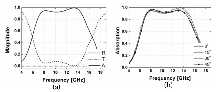
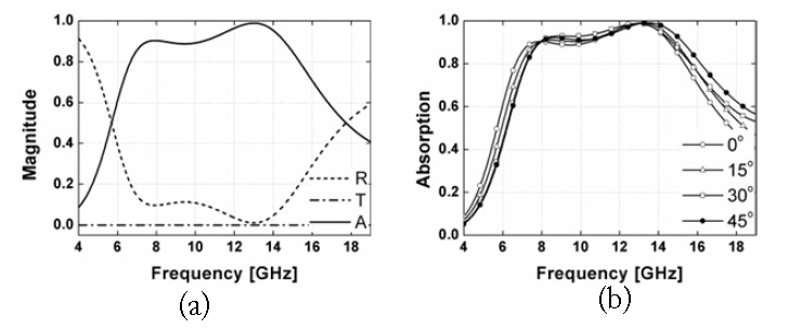
    Fig. 2 shows the EM-simulated results of the proposed absorber. We have used PEC boundaries on the top and bottom surfaces and used PMC boundaries on the side planes. For this kind of problem, the boundary condition used for a single unit is almost equivalent to using a Floquet port. As shown in Fig. 2(a), the metallic back plane ensures that the transmission is zero (T = 0). The reflection (R), transmission (T), and absorption (A) are related to the S-parameters via the following general relations:

    image

    For this work, T = 0. The maximum absorption rate is 99.5% at 13.3 GHz. The full width at half maximum (FWHM) is 95% at 11.2 GHz (5.9–16.5 GHz).

    Based on 90% absorption (A), the bandwidth is 66.7% at 10.95 GHz (7.3–14.6 GHz).

    Fig. 2(b) shows the absorption (A) of the proposed absorber depending on polarized angles of the electric field from the vertical direction. The absorption varies only slightly up to the investigated polarization angles of 45°. Due to the symmetry of the proposed structure, this result ensures that the proposed absorber is insensitive to incident fields having any polarization angles.

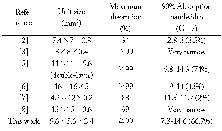
    In Table 1, we compare the absorption characteristics of the proposed absorber with those of others in terms of size, peak absorption, and 90% absorption bandwidth. Although a doublelayered absorber in [5] shows a substantial wideband characteristic, the absorption characteristics of this design with a single layer seem to be fairly good.

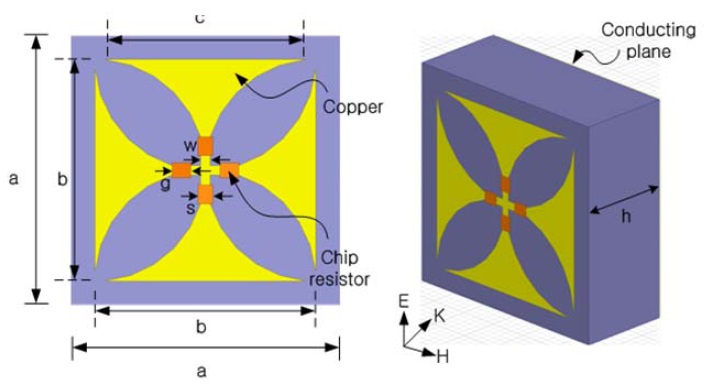
    Fig. 3 shows the geometry of the proposed absorber with a resistive surface pattern having a uniform surface resistance per square (case 2). The optimized dimensions of the proposed unit cell are: a = 5.6 mm, b = 4.6 mm, c = 4.2 mm, w = 0.2 mm, h = 2.4 mm. The surface pattern has been optimized by 7 Ω/square.

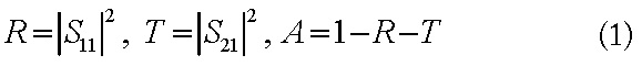
    Fig. 4 shows the EM-simulated results of case 2. As shown in Fig. 4(a), the maximum absorption rate is 99% at 13 GHz. The FWHM is 102.8% at 11.7 GHz (5.7–17.7 GHz). The 90% absorption bandwidth is 64% at 11.6 GHz (7.9–15.3 GHz).

    [Table 1.] Comparisons of absorption characteristics between the proposed absorber and others

    label

    Comparisons of absorption characteristics between the proposed absorber and others

    Fig. 4(b) shows that case 2 also maintains similar polarization insensitivity to that seen in case 1.

    III. CONCLUSIONS

    Two types of metamaterial-inspired wideband absorbers have been designed that adopt trumpet structures. The first one uses a copper surface pattern with chip resistors. The second one employs a uniform resistive surface pattern. Both types of absorbers are single-layered. The mechanism of wideband operations has been explained with simple and familiar circuit interpretation. Both designs show excellent wideband characteristics at the X-band, with high absorption. The proposed absorbers are also almost polarization-independent. In particular, the proposed absorber with uniform resistive pattern may facilitate mass production and may be adopted, for instance, to render combat aircraft invisible to X-band radars.

참고문헌
  • 1. Ye Q. W., Lin H., Chen X. Q., Yang H. L. 2011 “A tunable metamaterial absorber made by micro-gaps Structures” [in Proceedings of 2011 Cross Strait Quad-Regional Radio Science and Wireless Technology Conference] P.234-237 google
  • 2. Lee H. 2012 “Design of metamaterial absorber based on resonant magnetic inclusion” [in Proceedings of the 2012 International Symposium on Antennas and Propagation] P.1501-1505 google
  • 3. Campbell S. D., Ziolkowski R. W. 2013 “Lightweight, flexible, polarization-insensitive, highly absorbing meta-films” [IEEE Transactions on Antenna Propagation] Vol.61 P.1191-1200 google cross ref
  • 4. Fan Y. N., Cheng Y. Z., Deng Y. M., Gong R. Z. 2012 “Absorbing performance of ultrathin wide-band planar metamaterial absorber” [in Proceedings of the 2012 10th International Symposium on Antennas, Propagation & EM Theory] P.672-676 google
  • 5. Yoo M., Lim S. 2013 “Wideband metamaterial absorber using an RC layer” [in Proceedings of 2013 Asia-Pacific Microwave Conference] P.1227-1229 google
  • 6. Olszewsk M., Salski B., Gwarek W., Bajurko P., Yashchyshyn Y., Jakubowska M., Janczak D. 2013 “A broadband metamaterial absorbing panel with a resistive pattern made of ink with graphene nanoplatelets” [in Proceedings of the 43rd European Microwave Conference] P.1039-1042 google
  • 7. Landy N. I., Sajuyigbe S., Mock J. J., Smith D. R., Padilla W. J. 2008 “Perfect metamaterial absorber” [Physical Review Letters] Vol.100 google cross ref
  • 8. Lee J., Lim S. 2011 “Bandwidth-enhanced and polarisationinsensitive metamaterial absorber using double resonance” [Electronics Letters] Vol.47 P.8-9 google cross ref
OAK XML 통계
이미지 / 테이블
  • [ Fig. 1. ]  Geometry of the proposed absorber (case 1).
    Geometry of the proposed absorber (case 1).
  • [ Fig. 2. ]  EM-simulated results of the proposed absorber using chip resistors (case 1). (a) Reflection (R), transmission (T), and absorption (A). (b) A depending on polarization angles.
    EM-simulated results of the proposed absorber using chip resistors (case 1). (a) Reflection (R), transmission (T), and absorption (A). (b) A depending on polarization angles.
  • [ Table 1. ]  Comparisons of absorption characteristics between the proposed absorber and others
    Comparisons of absorption characteristics between the proposed absorber and others
  • [ Fig. 3. ]  Geometry of the proposed absorber using a resistive surface pattern with uniform surface resistance per square (case 2).
    Geometry of the proposed absorber using a resistive surface pattern with uniform surface resistance per square (case 2).
  • [ Fig. 4. ]  EM-simulated results of the proposed absorber with resistive pattern (case 2). (a) Reflection (R), transmission (T), and absorption (A). (b) A depending on polarization angles.
    EM-simulated results of the proposed absorber with resistive pattern (case 2). (a) Reflection (R), transmission (T), and absorption (A). (b) A depending on polarization angles.
(우)06579 서울시 서초구 반포대로 201(반포동)
Tel. 02-537-6389 | Fax. 02-590-0571 | 문의 : oak2014@korea.kr
Copyright(c) National Library of Korea. All rights reserved.