Graphene–a single atomic layer of graphite–has been in the scientific spotlight ever since its discovery in 2004 [1]. After a decade of substantial research, its electrical, optical, and mechanical properties are now better understood. In addition, various graphene-based labscale devices, such as electrodes [2-4], field-emitting devices [5,6], and sensors [7,8], have been successfully fabricated. Although these accomplishments show a glimpse of the promising technology graphene could bring in the future, there are still many hurdles that needs to be overcome before graphene becomes incorporated into our everyday devices.
Various methods have been assessed in an effort to produce graphene on an industrial scale. These include chemical exfoliation [9], epitaxial growth on SiC [10], and chemical vapor deposition (CVD). The chemical exfoliation method can produce graphene inexpensively, but the intrinsic properties of graphene produced by this method are very poor due to the vast amount of defects created during the harsh chemical treatment. On the other hand, the epitaxial growth on SiC produces graphene with much better intrinsic properties. However, the growth of graphene takes place on an expensive SiC substrate, making it unfeasible for large-scale production. CVD overcomes the drawbacks of these methods with its use of inexpensive substrates such as Cu and Ni, where the dimensions of graphene are only limited by the size of the substrate placed in the system.
The very first CVD graphene system was reported in 2008/2009 [11,12]. At that time, single- and multi-layer graphene were grown on Ni substrates. Since then, the drive to create predominantly monolayer graphene has continued. By controlling different variables, researchers began to understand the conditions required for monolayer growth. Furthermore, the roll-to-roll (R2R) production of predominantly monolayer graphene film reaching 30 inches was achieved by Bae
Since the predominant monolayer growth of graphene was realized, the research directions with regard to CVD graphene sought either to improve the quality of graphene or to make it more viable for mass production. To improve the quality of graphene, researchers mainly looked into improving its electrical aspects, as it was these aspects that made graphene such a popular subject. It was found that defects induced during the transfer processes [14] and the polycrystalline nature of CVD graphene hampered the electrical properties of graphene [15]. To make it more viable for mass production, approaches to eliminate the need for an etching step of a catalytic substrate, to enable the low-temperature growth of graphene, and to realize the aforementioned R2R production of graphene [13,16,17] were investigated. Producing large samples of graphene film is relatively straightforward, as doing so can be achieved by placing a larger Cu substrate in the CVD system on which the graphene can grow. However, etching the large Cu substrate and handling the transfer of the resulting large graphene sheet are difficult, as the conventional poly(methyl methacrylate) (PMMA) support transfer method cannot be used.
The major obstacle hindering the integration of graphene into our everyday devices has less to do with graphene production methods and more to do with the quality of the graphene that is produced. As mentioned above, the R2R production of 30- inch graphene sheets transferred to a target substrate has been achieved. However, the electron mobility of the graphene sheet was ~5000 cm2V-1S-1. Considering that the electron mobility of suspended graphene is ~200 000 cm2V-1S-1 [18] and that the electron mobility of graphene on SiO2 is ~40 000 cm2V-1S [19], it can be seen that much room for improvement still exists.
As mentioned earlier, the main reason behind the poor mobility value is most likely the defects that are induced during the transfer and the polycrystallinity of CVD graphene; however, the latter source contributes more to a reduction in the electron mobility. As Yu
2. Basic Factors That Change the Nucleation of Graphene
Before looking into methods proposed by researchers to grow large single-crystal graphene domains, the parameters that alter the nucleation of graphene will be investigated. In the CVD process, the controlled parameters are the substrate, the temperature, the pressure, and the gas composition. The growth time is another parameter that can be controlled in the CVD process, but it only affects the graphene coverage on the substrate. For this reason, this factor will be omitted here.
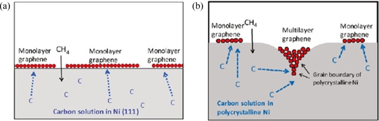
The substrate acts as a catalyst on which graphene can grow. Therefore, it is unsurprising that the substrate has a major influence on the nucleation of graphene. CVD graphene growth on various transition metals has been reported, such as Pt [21], Ir [22], Ni [11,12], and Cu [23], with the latter two favored due to their low cost. There are two different growth mechanisms of graphene: segregation growth and surface growth [24]. Segregation growth generally takes place on metals with high levels of carbon solubility, such as Ni. At high temperatures, carbon can dissolve into the bulk of Ni and segregate to the surface during cooling. In addition, carbon tends to segregate more at the grain boundaries of Ni (Fig. 2). Due to this phenomenon, graphene growth on Ni generally results in patches of multilayer growth, and limiting the growth to one layer is difficult. On the other hand, surface growth takes place on metals with low levels of carbon solubility, such as Cu. With Cu, carbon does not precipitate into the bulk of the metal and growth is limited to surface diffusion; given that growth only occurs at the surface, the growth of graphene terminates once the Cu is covered with graphene in what is generally termed “the self-limiting effect.” Therefore, once the Cu surface is covered with graphene, no further growth should take place. Thus, limiting the growth of graphene to a single layer becomes a much easier task. As a result, the most common type of substrate used for CVD graphene is a Cu substrate.
It should be noted that millimeter sized single-crystal graphene growth has been successfully achieved through segregation growth on Ni [26] and Ru [27]. However, additional processes were required to optimize the substrate, making it less desirable than Cu.
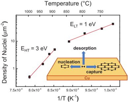
The most commonly reported temperatures for the monolayer growth of graphene on Cu range from 1000℃ to 1050℃. In this temperature range, complete coverage with predominantly monolayer growth is achieved for reasons that will be explained later in this section. Below this temperature range, incomplete coverage is observed even after a prolonged period of growth [28]. Also, the growth temperature can be as high as 1085℃, at which the Cu substrate reaches its melting point. Higher growth temperatures are favored to produce a large graphene domain size because increasing the growth [28]. This indicates that graphene can nucleate more easily in a low-temperature regime than in a high-temperature regime. For this reason, a high nucleation density is observed at low temperatures. temperature decreases the nucleation density of the graphene, allowing larger graphene domain growth (Fig. 3). At first glance, this may be slightly confusing, as one may expect the opposite to occur, as the activation energy for nucleation will be more easily met. However, it will be mentioned later that graphene prefers to nucleate in certain sites such as the grain boundaries, step edges, and other defect sites [29] and that increasing the temperature decreases the numbers of such sites. As a result, a reduction in the nucleation density is typically observed. Furthermore, the diffusion rate increases with the temperature; thus, the mobility of the carbon adatoms increases with the temperature. As the mobility of carbon adatoms increases, the probability that carbon adatoms will adhere to the existing graphene nucleus becomes greater than that of carbon adatoms creating a new graphene domain. An increase in the diffusion rate will also contribute to an increased growth rate of graphene domains, which in turn results in better growth coverage [30]. Kim
CVD can be classified into the following two categories according to the pressure: low-pressure CVD (LPCVD) and atmospheric- pressure CVD (APCVD). In LPCVD, the chamber is pumped down and maintained in the mTorr range before the reactant gases are introduced. In APCVD, the chamber is purged with Ar before the reactants gases are introduced.
To understand how the nucleation mechanism changes depending on the pressure, the deposition sequence needs to be understood. The deposition sequence of the typical CVD process is as follows:
1) Diffusion in of reactants through the boundary layer2) Adsorption of reactants on the substrate3) Chemical reaction occurs4) Desorption of the adsorbed species5) Diffusion out of by-products
The pressure essentially governs step 1 of the CVD process. When the pressure decreases, the gas flow rate in the CVD system increases. This, in turn, decreases the boundary layer thickness, as it is governed by the following equation [31]:
Here, Δ is the boundary layer thickness, x is the distance from the inlet, Re is the Reynold’s number, ρ is the fluid density, ux is the flow density, and μ is the viscosity.
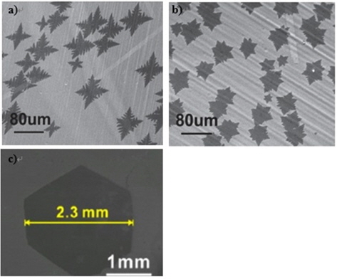
As a result, at LP, the boundary layer becomes thin and the diffusion of the reactant gas through the boundary layer becomes rapid, while at a high pressure, the boundary layer becomes thick and the diffusion of the reactant gas through the boundary layer becomes slow. Therefore, the pressure essentially controls the growth kinetics of nucleation. When the diffusion of the reactant gas through the boundary layer is fast, the growth rate is said to be controlled by the surface reactant kinetics. On the other hand, when the pressure is high, the boundary layer is thick, resulting in the slower diffusion of the reactants onto the substrate. Here, the growth rate is said to be controlled by diffusion or mass transport [31]. The different growth kinetics depending on the pressure determines the growth shape of the graphene domains. Typically, when growing graphene via APCVD, the expected hexagonal domain shape is observed (Fig. 4c), while when growing graphene via LPCVD, a completely different four-lobe or six-lobe graphene domain is observed (Figs. 4a and b). However, one perplexing point is that, despite the fact that growth via LPCVD tends to be controlled by surface reactions, the four- /six-lobe domains show dendritic growth. Dendritic growth is a sign that diffusion-controlled growth is occurring [34]; therefore, some other factor must be contributing to the growth kinetics during LPCVD growth.
The H2:CH4 gas ratio has important implications not only during the nucleation of graphene but also on the growth rate of graphene. Thus, the role of each gas will be examined independently before an explanation of how the H2:CH4 ratio affects growth.
CH4 is the most commonly used carbon precursor due to its relative abundance and low cost. Although the use of Cu substrates leads to self-limiting behavior of graphene growth, proper control of the CH4 flow rate is still required. For any nucleation to occur, supersaturation is required [35]; thus, the CH4 partial pressure needs to exceed this supersaturation point before the growth of graphene can be observed. As the partial pressure of CH4 increases further, the number of carbon adatoms able to attach to the existing graphene domains increases, causing the graphene growth rate to increase as long as sufficient diffusion is occurring. Also, once the supersaturation point is reached, nucleation will either occur or not occur depending on whether the energy barrier can be overcome, which is independent of the CH4 partial pressure. Thus, increasing the CH4 partial pressure has no effect on the nucleation density past the supersaturation point. However, if the CH4 partial pressure is too high, bilayer and multilayer graphene may form [36]. Thus, a certain parameter exists for graphene growth on Cu substrates to be self-limiting, which seems to be closely related to the partial pressure of CH4. In the case of LPCVD growth, a bilayer graphene island is always located near the center of a larger single-layer graphene island, hinting at the possibility of the bilayer graphene island acting as a seed [37,38]. To understand the initial nucleation of graphene further, Kalbac
Hydrogen also plays an important role in the nucleation of graphene [39]. In fact, hydrogen plays an important role in all three stages of graphene growth: pre-growth, growth, and after growth. In the pre-growth stage, hydrogen removes any oxygen impurities from the Ar carrier gas as well as oxide impurities on the metal catalyst surface [38]. Also, when CH4 is pumped into the CVD system, hydrogen helps decompose CH4 into carbon atoms. The carbon atoms then absorb and diffuse through the Cu to form graphene. During the growth of graphene, hydrogen controls the size and morphology of the graphene domains. A study by Vlassiouk
Altogether, the balance between CH4, which “creates” graphene, and H2, which “destroys” graphene, will dictate the growth rate of graphene. Thus, the fine tuning of the H2:CH4 ratio becomes important, not as much to control the nucleation density of graphene but to control the growth rate of graphene.
3. Tactics to Reduce the Nucleation Density
The previous section covered parameters that change the nucleation of graphene. However, how are these parameters implemented to grow large graphene domains? In order to achieve large graphene domains, the nucleation density needs to be suppressed such that “single-crystal” graphene grows as large as possible before its growth becomes terminated by the neighboring graphene domain, which in turn reduces the number of grain boundaries and hence improves the overall electrical properties of graphene.
The surface morphology of the Cu substrate plays an important role in the nucleation of graphene. For example, Liu
Another pretreatment that is often employed is to extend the pre-growth annealing of the Cu substrate. As mentioned in Section 2, graphene has a tendency to nucleate at defect sites such as the grain boundaries of Cu and other impurity sites. Because long-term annealing at elevated temperatures promotes grain growth and the recrystallization of the Cu substrate, it reduces the number of possible nucleation sites for graphene [36,46]. Wang
In another aspect, Kim
Nevertheless, millimeter-sized graphene domains have successfully been grown on polycrystalline Cu substrates, demonstrating that there are other factors that prevail and that the polycrystallinity of Cu may not be as daunting of an issue as initially considered.
For some researchers, annealing is not enough, and they took a step forward by completely melting the Cu substrate altogether. Wu
3.3. Non-reducing pre-growth atmosphere
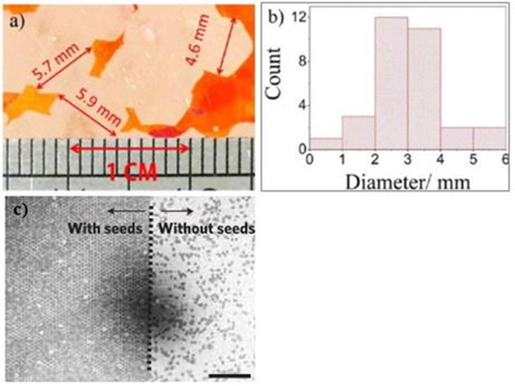
Another strategy used to limit the nucleation density and, hence, grow large graphene domains is to heat the substrate in a non-reducing atmosphere. Generally, during the heating of a CVD system to the growth temperature, both hydrogen and argon are flown into the CVD system - argon to create an inert atmosphere and hydrogen to remove oxide impurities in the Ar carrier gas and on the Cu substrate. However, simply by removing hydrogen from the heating step, a vast reduction of the nucleation density can be observed [20,58]. Using this strategy, Gan and Luo [58] reported graphene domain sizes as large as 5.9 mm and a nucleation density as low as 0.6 nuclei/mm2. A closer examination showed that an Ar-only environment produced a rough but uniform surface with copper oxide nanoparticles randomly distributed on the surface. These copper oxide nanoparticles were reduced to Cu during Ar:H2 pre-growth annealing, where graphene preferred to nucleate. Hydrogen is well known to be capable of reducing native oxide impurities on Cu substrates, such as CuO and Cu2O, to pure Cu [59]. However, why graphene prefers to nucleate in reduced Cu is not well understood. Gan and Luo [58] explained that graphene tended to nucleate in reduced Cu because it produced nanoparticles with heights as high as 50 nm. As these sites protrude mostly out of the Cu surface, the likelihood of carbon adatoms being captured increases. Moreover, increasing the pre-growth annealing time increases the number of reduced-oxide nanoparticles, whereas the number of particles taller than 20 nm decreases, and only those which are taller than 20 nm act as nucleation sites [58]. Thus, although increasing the annealing time increases the number of oxide nanoparticles, those which contribute to graphene nucleation decrease.
Zhou
3.4. Pressure and other tactics
In Section 2, we covered how the pressure effects the nucleation of graphene, but not much was mentioned on how it affects the nucleation density of graphene. Vlassiouk
Another indirect effect pressure has is the sublimation of Cu. Generally, graphene CVD takes place at 1000℃, which is close to the melting point of Cu (1084℃ [62]). Although the melting of Cu does not take place during the CVD of graphene, orangebrownish tainting on the quartz tube surface is often seen, which is evidence of Cu sublimation [63]. Vlassiouk
Another tactic that can be employed is initially to raise the carbon concentration above the supersaturation point so that some nucleation will occur and then decrease the carbon concentration to below the supersaturation point so that further nucleation is inhibited while the growth of the existing graphene domain continues. Wu
4. Addressing the Issue of Homogeneity
Despite the efforts to reduce the nucleation density, random distributions of nucleation sites are inevitable (Fig. 7a). This causes the nucleation density to vary from area to area within the same Cu substrate. This can lead to a new problem in which too much variation of the graphene domain size can result in inhomogeneous graphene in which some areas have outstanding electric mobility (because clusters of large graphene domains exist and, hence, less scattering occurs), while other areas of the same sample have lower electric mobility. To avoid this phenomenon, seeding growth of graphene may be a solution. To the best of our knowledge, only two reports show arrays of graphene domain nucleation through a seeding mechanism [15,56]. With nucleation seed arrays, inhomogeneous graphene can be avoided as long as graphene nucleation starts at the nucleation seed arrays. Then, the nucleation density will be even throughout the entire area, and large variations in the electric mobility of the sample will likely be minimized. Yu
5. Outlook & Future Considerations
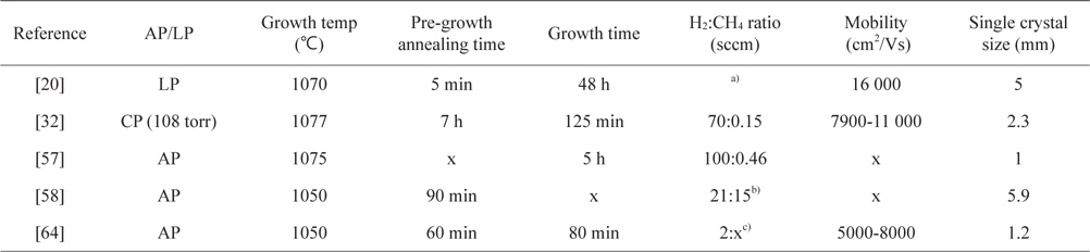
Ultimately, in order to incorporate CVD graphene into highend electronic devices, a large single-crystal graphene domain is needed. This is evident from electronic devices adopting singlecrystal silicon rather than polycrystalline silicon due to its higher performance. The trend shows that, by increasing the grain size of graphene domains, its property improves as well. Therefore, it is inevitable that growing large-size single-crystal graphene domains is important. However, vastly sacrificing the growth rate of graphene to achieve a large graphene domain will not help graphene become implemented in mainstream electronics, especially when growth and annealing processes lasting dozens of hours are necessary. For example, domain growth of 1 mm of graphene may be a great accomplishment, but if it requires a growth time of 48 h, it is unrealistic to be adapted for industrial- scale production [20]. Table 1 shows that most graphene domains over 1 mm require lengthy annealing and growth times. In addition, full graphene coverage is not achieved, even after those long hours. In this regard, researchers appear to get too carried away to create large single-crystal graphene domains, and they deviate too far from realizing a single-crystal graphene domain for mass production. Nevertheless, understanding the factors that influence the production of a large graphene domain size is invaluable, and these can always be altered to make mass production more feasible. It should always be kept in mind that the advantage of the CVD process is that large-area monolayer graphene can be grown, especially when the R2R potential has already been established [17].
[Table 1.] Summary of the parameters used for growth of millimeter-sized graphene domains

Summary of the parameters used for growth of millimeter-sized graphene domains
This review presents a current overview of research trends related to CVD graphene. Despite the realization of the R2R production of graphene films reaching 30 inches in length, the electronic properties were degraded due to the polycrystalline nature of the graphene produced. Thus, the need for large single-crystal graphene domains arose. To achieve large single-crystal graphene domains, the nucleation density had to be suppressed such that the growth did not terminate due to neighboring graphene domains. Basic factors that affected nucleation were looked into before the tactics used by researchers were reviewed. Despite the achievement of a relatively large domain size, it is difficult to employ the proposed strategies for mass production, as the growth and annealing times required to grow these large graphene domains are unfeasible. Also, the problem of an inhomogeneous distribution of these large graphene domains causing local variation of the properties within the same sample will need to be investigated in the future.

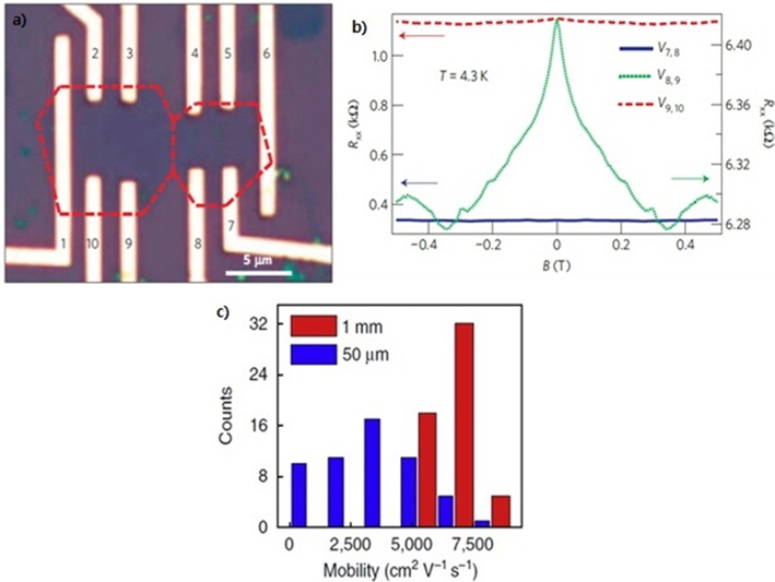
![(a) Electrodes patterned on neighboring graphene domains. (b) Graph showing the electrical resistance peaking at the inter-grain area (green line) compared to no electrical resistance change at the intra-grain area (blue and red lines). Reprinted with permission from [15]. Copyright ⓒ 2011, Macmillan Publishers Ltd. (c) Histogram of the carrier mobility distribution of graphene field-effect transistors made on a single-crystalline domain (red) and on polycrystalline graphene (blue). Reprinted with permission from [20]. Copyright ⓒ 2013, Macmillan Publishers Ltd.](http://oak.go.kr/repository/journal/13502/HGTSB6_2014_v15n3_151_f001.jpg)
![Schematic showing why the complete monolayer growth of graphene is difficult when segregated growth occurs. Reprinted (adapted) with permission from [25]. Copyright ⓒ 2010, American Chemical Society.](http://oak.go.kr/repository/journal/13502/HGTSB6_2014_v15n3_151_f002.jpg)
![Graph showing two temperature regimes with different activation energies. Reprinted (adapted) with permission from [28]. Copyright ⓒ 2012, American Chemical Society.](http://oak.go.kr/repository/journal/13502/HGTSB6_2014_v15n3_151_f003.jpg)
![(a and b) Scanning electron microscope (SEM) images of four-/ six-lobe flower graphene domains grown in the low pressure condition. Reprinted with permission from [33]. Copyright ⓒ 2013, Wiley. (c) SEM image of hexagonal graphene domain grown in the atmospheric pressure condition. Reprinted (adapted) with permission from [32]. Copyright ⓒ 2012, American Chemical Society.](http://oak.go.kr/repository/journal/13502/HGTSB6_2014_v15n3_151_f004.jpg)
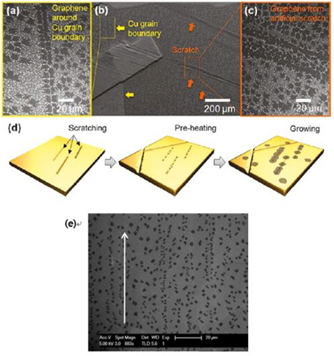
![(a-c) Scanning electron microscope (SEM) images showing graphene preferentially nucleating along the Cu grain boundary and an intentionally introduced scratch mark. (d) Depiction of graphene nucleating at the scratch mark shown in Figs. 5b and c. Reprinted (adapted) with permission from [43]. Copyright ⓒ 2011, American Chemical Society. (e) SEM image showing graphene preferentially nucleating along the rolling marks of Cu; the white arrow indicates the direction of the rolling marks. Reprinted with permission from [42]. Copyright ⓒ 2011, Elsevier.](http://oak.go.kr/repository/journal/13502/HGTSB6_2014_v15n3_151_f005.jpg)
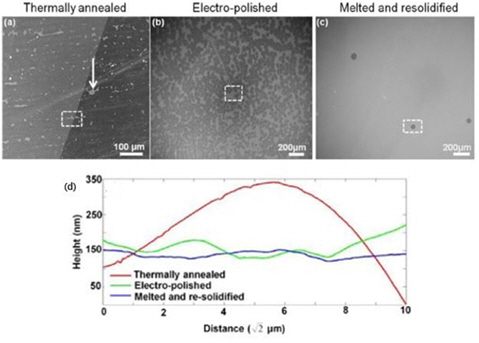
![(a-c) Scanning electron microscope (SEM) images showing the difference in the nucleation density of graphene between (a) thermally annealed Cu, (b) electro-polished Cu, and (c) melted and resolidified Cu. (d) Typical atomic force microscopy line profile of a thermally annealed, electro-polished and melted, and resolidified Cu substrate. Reprinted (adapted) with permission from [57]. Copyright ⓒ 2013, American Chemical Society.](http://oak.go.kr/repository/journal/13502/HGTSB6_2014_v15n3_151_f006.jpg)
![(a) Large graphene domains on a Cu substrate made visible by oxidization in air at 200℃ for 1 min, (b) graphene domain size distribution in (a). Reprinted (adapted) with permission from [58]. Copyright 2013, American Chemical Society. (c) Difference in the graphene nucleation distribution between seeded growth and non-seeded growth conditions. The scale bar corresponds to 200 μm. Reprinted with permission from [15]. Copyright ⓒ 2011, Macmillan Publishers Ltd.](http://oak.go.kr/repository/journal/13502/HGTSB6_2014_v15n3_151_f007.jpg)