Solid oxide fuel cells (SOFCs) exhibit great potential for solving the energy crisis and environment pollution, through offering a low-pollution technology to chemically generate electricity with high efficiency [1]. However, long-term stability, cost effectiveness, and large-scale production and commercialization of thin film electrodes and electrolytes require reduction of the operating temperature, whilst maintaining high electrocatalytic activity for low temperature SOFCs. But the reduction of the SOFC operating temperature causes several problems, such as ohmic drop through the electrolyte, and electrode overpotentials. Electrolyte materials with higher ionic conductivity are needed, in order to improve the SOFC efficiency at lower operating temperatures. This can be achieved by reducing the thickness of the electrolyte [2]. Although the typical electrolyte material is cubic ZrO2 doped with approximately 8 mol% Y2O3 (yttria stabilized zirconia-YSZ) [3], the reduction in working temperature leads to insufficient ionic conductivity. Ceria based electrolytes are more attractive in terms of conductivity at low temperature, but it is well known that these materials are reducible at very low oxygen partial pressure [4-6]. One main limitation of the GDC electrolyte is its mixed ionic and electronic conduction (MIEC), i.e., higher electronic conductivity with decreasing theoretical voltage, caused by the reduction of ceria from Ce4+ to Ce3+ from the anode side, where the electrolyte is exposed to a reducing atmosphere. This is the reason they are protected by an electron blocking layer, to avoid cell efficiency losses. One effective approach reported in bulk electrolyte structure is to incorporate YSZ as a blocking layer in between the GDC and anode, to inhibit chemical reduction of GDC and electrical current leakage [7-10]. Therefore, to achieve the optimum cell performance of bilayer electrolyte cells, it is necessary to optimize the YSZ thickness. Recent progress in technology allows building anode supported dense electrolytes of only several micrometers thick; thus, electrolyte resistance can be significantly lowered [11]. Electrolyte thin films could be prepared by vapor processing methods (such as chemical vapor deposition (CVD), electrochemical vapor deposition (EVD), metalorganic CVD (MOCVD), sputtering, plasma spray, etc.). Despite these challenges, vacuum methods offer a number of unique advantages. In this work, we demonstrate a well designed bilayer GDC/YSZ electrolyte structure using a thin film approach, where the thickness of the YSZ layer is carefully controlled, to explore the effect of YSZ thickness on the overall performance of the bilayer electrolyte cells. Using this approach, it is possible to identify the optimum YSZ interlayer thickness that effectively suppresses a significant, without reducing the ionic conductivity in the GDC electrolyte.
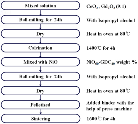
2.1 Fabrication of NiO-GDC anode substrate
Ni-GDC anode powders were synthesized by solid-state reaction method, using appropriate oxide materials. Cerium oxide (CeO2), Gadolinium oxide (Gd2O3) and Nickel oxide (NiO), all with purity above 99% (Aldrich, USA), were used as reagents. The flowchart of Fig. 1 summarizes the fabrication process. The CeO2 and Gd2O3 mixture starting materials in the composition Ce0.9 Gd0.1O1.9 were mixed sufficiently, and ball-milled for 24 h with isopropyl alcohol (IPA). After the mixture was dried at 80℃, this powder was calcined in air at 1,400℃ for 4 h. The selection of the ceramic composition of NiO60-GDC40 (precursor composite for Ni-GDC anode) substrate was decided on the basis of its viability in prospective use as an anode of half-cell for IT-SOFC [12,13]. The calcined GDC powder was then reground, and mixed with NiO in the desired proportion, to obtain the composite phase of composition of NiO60-GDC40, by ball-milling for 24 h. The binder added powder was pelletized with the help of a press machine. The green samples were then sintered at 1,600℃ for 4 h in air. The pre-sintering (binder removal step) of samples was intentionally excluded, as the high sintering temperature is usually employed to obtain dense ceramic bodies, and here we are expecting porous structured (anode-grade) NiO-GDC substrates. The dimensions of the sintered substrates were 0.15 cm in thickness and 2.0 cm in diameter.
2.2 Preparation of GDC/YSZ bilayer thin film
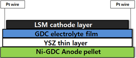
The GDC/YSZ bilayer thin film was deposited on NiO-GDC substrate. This was cleaned in an ultrasonic bath of acetone, ethanol solution, and distilled water for 3 min each, before RF sputtering and E-beam evaporation. Bilayers constituted by YSZ coating were sputter deposited by RF sputtering of Zr-8 at.% Y target, 2 inch in diameter, in argon-oxygen reactive mixtures. The experimental device is a sputtering chamber pumped down via a turbo molecular pump, allowing a base vacuum of 4.5 × 10⁻⁶ Torr. Argon and oxygen flow rates were controlled by MKS flowmeters, and the pressure was measured by an absolute Baratron gauge. The substrates were positioned on a substrate holder at the draw distance of about 100 mm. YSZ thin layers were first sputterdeposited onto the NiO-GDC substrate, under an oxygen : argon mixed atmosphere (2.5 : 40 sscm). The total pressure in the chamber varied slightly from 0.77 to 0.74 Pa. These GDC layers were next covered by a YSZ layer. The evaporation experiment was performed in a vacuum of 4.5 × 10⁻⁷ Torr. The gun power in the e-beam process was 1.05 kW, and the deposition rate was controlled by adjusting the gun power. Substrates were heated at 400℃. Fig. 2 is a schematic of the single cell configuration.
The crystal structures of the electrolyte thin films were analyzed using X-ray diffraction (XRD) (D/MAX-2200, Rigaku) with the Cu Ka line. The XRD was operated at 40 kV/20 mA in the range of 2 w= 20~80, with a scanning speed of 0.02 2i/min. Surface and cross-sectional morphology were examined by field emission scanning electron microscopy (FESEM) (Model S-4700, Hitachi). The ionic conductivities of the GDC thin films were measured with a 2-probe ac impedance method, using an impedance analyzer (Solartron 1255B). The impedance spectra were obtained for the frequency range of 0.1 Hz~100 kHz, at temperatures from 773 to 1,073 K, in H2 and O2. For the impedance measurement, a Pt electrode was painted by screen printing method onto the substrate, and then electrolyte film was deposited on the Pt electrode.
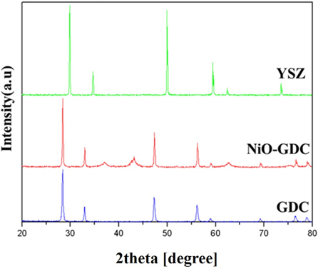
The GDC electrolyte and NiO-GDC anode substrate were synthesized by a solid state reaction method. In Fig. 3, the X-ray diffraction (XRD) pattern of electrolyte layer represents a typical cubic fluorite structure, and sharp lines repeat the crystal structure of the evaporating bulk electrolyte powder used in this study, which indicates that a single solid solution of Gd2O3-doped CeO2 is formed, after sintering at 1,400℃ for 4 h. The phase analysis of these YSZ thin films was done using XRD technique. The crystalline structure of the YSZ thin film after sintering was examined by X-ray diffraction, as shown in Fig. 3. This pattern shows that the deposited YSZ films were fully stabilized in the cubic phase [14]. YSZ thin films were deposited on porous Ni-GDC substrate by RF-sputtering. To obtain stable YSZ thin films on the porous Ni-GDC substrate, the influence of process parameters was examined. YSZ thin films were successfully prepared at optimized deposition conditions, with temperature of 400℃.
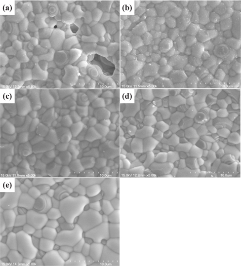
Figure 4 shows the effect of the microstructure YSZ layer samples. The gun power in the RF-sputtering process was in the range of 80 to 200 W. Figures 4(a) and (b) show surface views of the YSZ layers deposited at the RF gun power range of 80 W and 120 W, respectively. In Fig. 4(a), open pores can be observed in the figure, and some closed pores are also visible. But the micrograph of Fig. 4(b) establishes the existence of dense structure. No open pores can be observed in the figure, although some contamination is evident. Figures 4(c) and (d) show that as the gun power increases, a dense film structure is established. At this point, we estimated that the characteristics of the thin film had improved the density, by increasing the gun power.
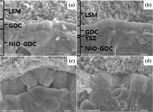
Figure 5 shows surface view and cross-sectional view SEM micrographs of anode supported single cells. The microstructures of both the~2 μm GDC single layer (Fig. 5(a)) and GDC/ YSZ bilayer electrolyte (Figs. 5(b)~(d)) show dense layered structures between the cathode and anode electrodes. It is obvious that the electrolyte layers remain dense and solid after the high temperature measurements, and the adhesion between the adjacent layers is excellent, without any obvious crack formation at interfaces. Based on the above microstructural, electrochemical, and power measurement results, it is evident that a tailored bilayer electrolyte is needed for the optimization of power density characteristics and electrolyte stability, i.e., a bilayer electrolyte structure with proper YSZ thickness can enable chemical, mechanical, and structural stability of the YSZ/GDC electrolyte in single cells. Table 1 shows the bilayer thickness for the RF-sputtering gun power.
[Table 1.] Analysed samples, with their respective thicknesses of tGDC and tYSZ bilayer.
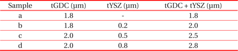
Analysed samples, with their respective thicknesses of tGDC and tYSZ bilayer.
The ionic conductivity of the electrolyte films was analyzed by a 2-probe ac impedance method, in the operating temperature range from 500℃ to 800℃. The electrode kinetics are very active at high temperatures, due to the increased operating temperature. The ionic conductivity was obtained from the following equation.
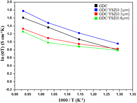
The Arrhenius plots of total conductivity versus reciprocal temperature shown in Fig. 6 are derived from the AC impedance spectra, for a comparison between the total conductivities of the GDC single layer and GDC/ YSZ bilayers, as a function of the YSZ film thickness. By increasing the YSZ thickness, the total resistance increases. The same behaviour can be deduced when the GDC layer is fixed, and YSZ varies from 0.2 μm to 0.8 μm. These observations were not verified by comparing the resistance evolution for GDC thickness. Thus, it seems that YSZ has more influence than the GDC layer. Although the AC impedance study shows a decrease of the electrical conductivity with YSZ incorporation (Fig. 6), it should be noted that the measurement was performed in air, where GDC remains as a pure oxide ion conductor. In actual single cell configuration, however, the GDC electrolyte will be reduced from the anode side in contact with fuels, which results in OCV loss, and consequent deterioration of the SOFC performance. Therefore, the effect of the GDC/ YSZ bilayer on the OCV and fuel cell performance has been evaluated using NiO-GDC anode-supported single cells.
We have successfully investigated the microstructural and electrochemical properties of GDC/YSZ bilayer electrolytes with YSZ thickness varying from ~0.2 μm to ~0.8 μm, for thin film SOFCs. The total conductivity of the bilayer films is found to be inversely proportional to the YSZ film thickness, at the intermediate operating temperatures in air. However, the single cells with GDC/ YSZ (0.2 μm thickness) bilayer electrolyte show conductivity comparable to that obtained with the GDC single electrolyte layer. The GDC/ YSZ bilayer electrolyte shows the effectiveness of YSZ as an electron blocking layer. YSZ plays a very important role in the electrical properties. In order to increase the total conductivity, not only must the thickness be reduced, but specific attention is required to optimise the thickness ratio between GDC and YSZ. A thorough analysis of each individual YSZ and GDC monolayer, with strictly the same electrochemical devices, synthesis conditions (RF-sputtering, and the same thicknesses as in the bilayered sample), is necessary.