Ballast is a device intended to limit the amount of current in an electric circuit. A familiar and widely used example is the inductive ballast used in fluorescent lamps, to limit the current through the tube, which would otherwise rise to destructive levels, due to the fluorescent tube’s negative resistance characteristic. Generally speaking, ballast can be categorized into two major types: electromagnetic ballast and electronic ballast. Compared with electromagnetic ballast, electronic ballast has some advantages, such as higher luminous efficacy, lighter weight, and the elimination of flicker and audible noise
Electronic ballast usually supplies power to the lamp at a frequency of 20 kHz or higher, rather than the mains frequency of 50~60 Hz [1]; this substantially eliminates the stroboscopic effect of flicker, a product of the line frequency associated with fluorescent lighting. The high output frequency of the electrical ballast refreshes the phosphors in a fluorescent lamp so rapidly that there is no perceptible flicker. With the higher efficiency of the ballast itself, and the higher lamp efficacy at higher frequency, electronic ballast offers higher system efficacy for low pressure lamp, like the fluorescent lamp.
Electronic ballast is often based on switch mode power supply (SMPS) topology, such as[m1] the ringing choke converter (RCC), push-pull inverter, half-bridge inverter and full-bridge inverter, which first rectify the input power, and then chop it at a high frequency. The gate-drive methods used for electronic ballast can be further categorized into two major types: self-exciting and ICcontrolled versions. The self-exciting converters have a long history, of more than 45 years, and find many applications in power supplies, such as dc-to-dc converters, and electronic ballast. The major advantages of self-exciting converters are circuit simplicity and robust operation. In electronic ballast application, the self-exciting inverter is regarded as one of the simplest and most cost-effective topologies. Disadvantageously, however, the operating frequency of the self-exciting circuit is, by the nature of its operation, load dependent; and thus is very difficult to control, and the driver waveform is affected by the power switch and selfexciting current transformer, causing high switching loss and high temperature, leading to the increase of heat dissipation area, and reduction of product reliability [1,2].
In this paper, a novel drive circuit of the self-exciting electronic ballast is proposed. The circuit employs BJT as a power switch, and a linear core for the current transformer. Firstly, the operation principle of the BJT-based typical self-exciting electronic ballast is analyzed, and the cause of high switching loss was found; meanwhile, experiment and simulation results are presented to validate the analysis. Then, the novel self-exciting electronic ballast is proposed. All switches in the novel circuit are soft switching, which is verified by the experimental and simulation results. Finally, based on the operational principle of novel self-excitation electronic ballast, how to choose and wind the magnet ring, and the design procedure, were provided in this paper.
2. TYPICAL SELF-EXCITING ELECTRONIC BALLAST
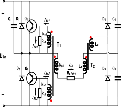
Figure 1 shows a typical circuit of BJT-based self-exciting electronic ballast. D1, D2, Q1, Q2, C3 and C4 make up a half-bridge topology. Two BJTs form a half-bridge inverter stage, to output a square voltage wave. The self-exciting drive circuitry is composed of a current-transformer, T1, with three windings (Np1, Ns1, and Ns2), and gate resistors Rbl and Rb2. The resonant inductor current is fed back through the T1, and converted into a complementary voltage, to drive the two BJTs, Q1 and Q2. The T1 is in series with the inductor L1. The polarities of the T1 are chosen in such a way that inductor current, flowing through the primary side of T1, will generate complementary gate drive voltages to the BJTs Q1 and Q2, causing the circuit to oscillate. An inductive appearance of the tank is naturally obtained by this configuration, so that zerovoltage switching (ZVS) is achieved for both BJTs. The inductor L1 limits the output current, and its coupling coil L2, D3 and D4 are employed, to reject the unbalancing problem of neutral-point voltage, due to the inconsistency of capacitors C3 and C4 in the half-bridge circuit [3-5].
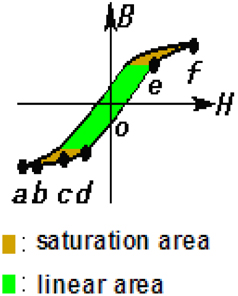
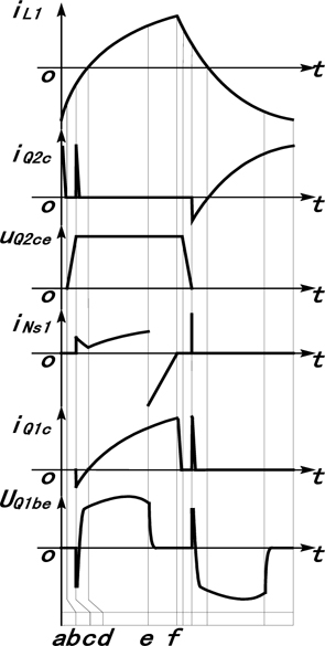
The key waveforms concerned are shown in Fig. 2, and the trajectory of the current-transformer T1 is shown in Fig. 3. The operational principle of the circuit is as follows:
1) Stage [a, b]: In this stage, the current injecting collector of Q2 becomes lower; meanwhile, C1 begins to discharge, and the junction capacitance CQ2ce of Q2 to be charged. At the end of this stage, as a result of the current injecting collector of Q2 quick declining, and the larger value of C1 and CQ2ce in parallel, the voltage across C1 is almost unchanged. It is assumed that the current of the inductor L1 remains unchanged, because of small timeinterval. The voltage of UQ1b-e and UQ2b-e are almost zero, since the current-transformer T1 is in deep saturation state, so the currents flowing from the windings Ns1 and Ns2 are close to zero. According to Ampere law,

where, H and lc are the magnetic field intensity, and the circumference of magnet ring T1, respectively. As a result, the absolute value of the magnetic field intensity reduces, and the corresponding operating point of magnet ring T1 moves from a to b.
2) Stage [b, c]: In this stage, C1 discharges, and the CQ2ce is charged by the current of inductor L1. At the end of this stage, the voltage across C1 is almost zero, and the voltage across CQ2ce is equal to Uin. During this time-interval, magnet ring T1 is still saturated, but begins to withdraw from deep saturation, and the absolute value of the magnetic field intensity continues to reduce, just like stage [a, b]. Hence, the corresponding operating point of the magnet ring T1 moves from b to c.
3) Stage [c, d]: At t=c, the inductor L1 remains discharged, and the current reduces to zero at the end. If assuming that D1 starts to conduct, UD1on is about 1.2 V. However, the magnet ring T1 is still saturated, UQ1b-e is almost zero, and the on-state voltage drop of p-n junction of Q1 is only 0.7 V. Obviously, the diode D1 is clamped, but the p-n junction provides a free-wheeling path, instead. During this time-interval, according to Ampere’s law, it is obtained that

Therefore, the absolute value of magnetic field intensity increases suddenly at the time of point c; then, with the current reduction of L1, the absolute value of the magnetic field intensity gradually decreases. According to Faraday’s law,

UQ1be is negative at the time of point c, and UQ1be is positive at the end, but UQ2be is opposite to UQ1be, which causes the sudden conduction of Q2. It is probable that the reverse recovery surge current flows through Q2 in several microseconds in this timeinterval; meanwhile, Q2 withstands the high dv/dt voltage [6]. Therefore, it causes high switching loss of BJT.
4) Stage [d, e]: At t=d, Q1 starts to conduct. The magnet ring T1 withdraws from deep saturation quickly, and operates in the linear area, due to the positive feedback effect. During this timeinterval, UQ1b-e is about 0.6 V, UQ1be divided by Rb1 equals iRb1, and iRb1 is about zero, and so is iRb2. According to Ampere’s law, it is obtained that


where, hef is the current gain of the transistor.
Meanwhile,

it is indicated that the magnetic flux increase linearly, until point e.
5) Stage [e, f ]: In this stage, the magnet ring T1 becomes saturated, so that UQ1b-e is about zero. Nevertheless, Q1 is still in the conduction state, because of the charge storage effect. At the time of point f, Q1 is off.
2.2 Simulation and experiment results
Take a fluorescent lamp GE F40/T12 for example. The output current is about 1.2 A, the output voltage is about 70 V, and the self-exciting frequency is about 22 kHz, applying the rated voltage of 220 Vac. The circuit parameters are:
DC link voltage Uin=300 V; Tank components: L1=1 mH, C3=C4=100 uF; T1 (TDK PC40 E116 Core): Np1 =3 T, Ns1=Ns2=4 T; Power transistor Q1 and Q2: BUV48A; Rated lamp power: 75 W;
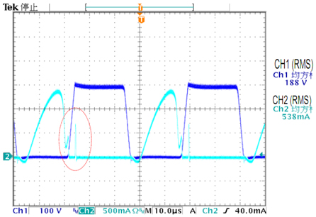
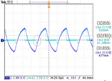
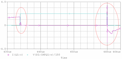
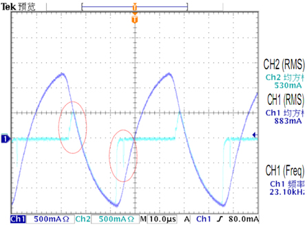
Switching waveforms are as shown in Fig. 4 using OrCAD10.5 software, and the experimental results are shown in Fig. 5 and Fig. 6, respectively.
It is proved true that the p-n junction of the transistor provides a free-wheeling path, and the transistor is suddenly turned on, causing high switching losses of the transistor.
3. NOVEL SELF-EXCITING ELECTRONIC BALLAST
Based on the above analysis and results, high switching loss and high temperature cause the increase of heat dissipation area and reduction of product reliability, owing to the coupling of gate-drive signals of upper and lower bridge arm, produced by the self-exciting transformer. To solve the above key problems, a novel circuit of electronic ballast is proposed in this paper.
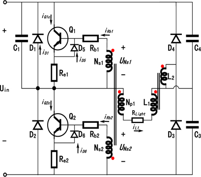
Figure 7 shows the circuit of novel self-exciting electronic ballast, and the key waveforms concerned are shown in Fig. 8, and the trajectory of the current-transformer T1 is almost the same as Fig. 3. The operational principle of the circuit is as follows:
The operational principle of the novel ballast in stage [a, b] and [b, c] are the same as typical self-exciting electronic ballast.
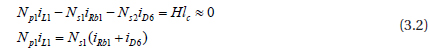
1) Stage [c, d]: Compared with the typical self-exciting electronic ballast, thanks to series resistance Rb1, both the diode D1 and p-n junction of Q1 provide a free-wheeling path in this stage. It can be seen that

At t=c, D1 is turned on, UD1 is about 1.2 V, and magnet ring T1 is still saturated. According to Ampere’s law and Faraday’s law, the same conclusions can be obtained that UNs1 is negative at the time of point c, UNs1 is positive at the end, and the current IRb1 increases. Owing to the placement of series resistance Rb1, the base current of Q2 is relatively small, and Q2 is kept off. In addition, thanks to the introduction of the two Schottky barrier diodes D5 and D6, as shown in Fig. 7, low impedance passes are provided for the flow of reverse base current, when the transistor is off [3]. It loosens the coupling between the gate-drive of each transistor, and makes the self-exciting magnet ring not very deeply saturated, resulting in easy commutation at the knee point of magnet ring [6].
2) Stage [d, e]: At t=d, Q1 starts to conduct. The magnet ring T1 withdraws from deep saturation quickly, and operates in the linear area, due to the positive feedback effect. During this timeinterval,
Assuming that iRb1 and iD6 satisfy the following equation,

it is obtained that

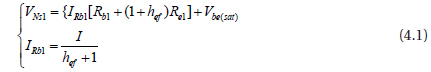
3) Stage [e, f]: During this time-interval, for the sake of saturation of the magnet ring, UNs1 is near zero, and the IRb1 current is given by

3.2 Simulation and experiment results
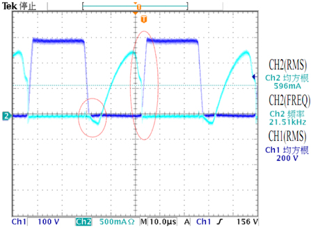
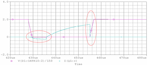
The simulation of switching waveforms of novel self-exciting electronic ballast are as shown in Fig. 9, and the experimental results are shown in Fig. 10 and Fig. 11, respectively.
Compared with Fig. 5, the collector current spike of the transistor is eliminated, as shown in Fig. 10; meanwhile, all switches in the novel circuit are soft switching, and the losses of the power switches are reduced, as shown in Fig. 11.
It is shown in the experiment that without a heat-sink, the collector temperature of the transistor is just 25℃ higher than the ambient temperature, meeting the project requirement.
Some assumptions are made, as follows [7-9]:
1) The self-exciting frequency is about 20 kHz. 2) The waveform of the tank current is a pure sine wave, and the rms is I. 3) The waveform of UNs1 is a pure sine wave.
It can be seen that:

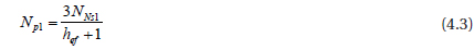
According to Faraday’s law, the winding turns of secondary coils can be expressed by the following formula [10]:
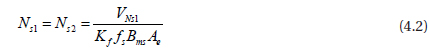
where, Kf is the wave coefficient, and equal to 4.44 as a pure sinewave, u is the core material permeability, Ae is the effective crosssection area, Bms is the operation magnetic flux density, and fs is the self-exciting frequency. Thus, the windings turns of primary coils can be calculated by

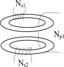
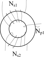
The following addresses the method of winding the self-exciting transformer, and three winding methods are shown in Fig. 12, Fig. 13, and Fig. 14.
The problem with the single-ring, as shown in Fig. 12, is that the turn-on waveform of one transistor is the exact inverse of the turn-off waveform of the other, so there is no possibility of driving them appropriately, and differently and efficiently.
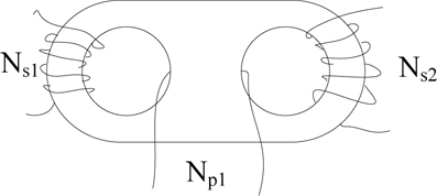
To conquer the limitations of the single-ring drive, the doublering approach could be used, as shown in Fig. 13. However, if the permeability and dimension of the two rings are not well matched, discrepancies during the crossover result in losses. It is advisable to use a balun-ring core to drive the transistors, as shown in Fig. 14 [11].
In addition, it is sensible not to select high relative permeability (greater than 6000) in the power ferrite material, which has poor performance in permeability under the temperature change [11].
A novel self-exciting electronic ballast is proposed, implemented and tested in this paper, and all power switches in this circuit are soft-switching. Moreover, how to choose and wind the magnet ring and the design procedure are provided in this paper. The proposed circuit is very simple, and ideal for low cost and high reliability self-exciting electronic ballast.