Semiconductor packaging technology is continuously developing for increased functionality and higher chip packing density, this is driven by the strong demand for smaller size, faster data communication, and greater storage capacity with increased reliability at lower manufacturing cost. To meet the desire for portable electronics products, microelectronics packaging technology has developed system-in-packing (SiP) for increased functionality and heterogeneous stacked chips for a higher chip density. With this trend in microelectronics packaging, one may have expected to observe the recent development of 3-D SiP for a multifunctional package module comprising of digital, RF, and memory functions [1].
Interconnecting technology in advanced semiconductor packaging for multi-layered or stacked memory device includes fine pitch-ball grid arrays (FP-BGA) [2], copper pillar tin bumping (CPTB) [3], through silicon vias (TSVs) [4], etc. The physical limitations of device shrinkage following Moore’ Law was alleviated by employing homogeneous chip stacking technology and heterogeneous chip interconnection in 3-D. Stacked-die chip scale packages (CSP) present challenges like wafer thinning and sawing, die attachment and spacer technology, as well as wirebonding with a smaller ball size and pitch. Despite this the technology offers functional integration in a minimal footprint, low cost, and good time-to-market for numerous microelectronics applications. Kamezos proposed the key factor of cost of ownership in their 3-D packages is not the cost of the module, but the final test yield [5].
Factors affecting final test yield in multichip stacking assemblies reside in all the challenges of wafer thinning and sawing, die attachment and spacer technology, and the wire-bonding process; however, this paper focuses on wire-bonding as a final yield lowering factor in conjunction with the previous step of wafer fabrication. During the gold wire-bonding process in NAND flash multichip package assembly processes, some weakly bonded wires on the aluminum bonding pads were observed and their most likely cause was identified as plasma etching of the bonding pad in the bonding pad opening process by extensive surface analysis of poorly or weakly bonded samples. The ball shear test (BST) and ball pull test (BPT) were performed on the sample under analysis, and various surface analysis, using X-ray photoelectron spectroscopy (XPS), Auger electron Spectroscopy (AES), and energy dispersive X-ray analysis (EDX), were performed to investigate contaminants on the bonding pad.
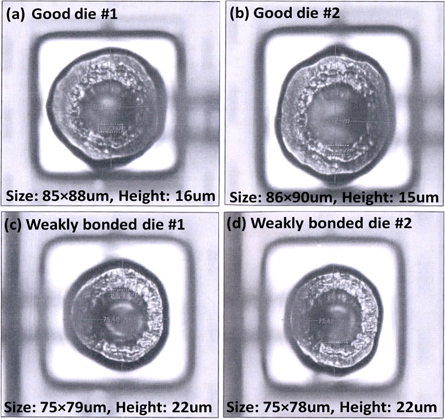
After increased requests for wire-bonding rework from the assembly line, 96 units were used as test vehicles for bonding strength measurement. In our initial trial, ball diameters vs. heights from both good dies and weakly-bonded dies were measured for visual comparison, and their microscopic images are presented in Fig. 1.
The shape of weakly-bonded dies is flatter in their height and have a wider bonding contact compared to those of good dies, this called for further investigation on the two types of samples employing the ball shear test (BST) and ball pull test (BPT). The BST is the most commonly accepted method for assessing the strength of wire-bonding or solder ball bonding, and the bond shear failure modes observed during the bond shear test include the following: (1) bond lift; (2) ball shear; (3) cratering; (4) bonding surface failure; (5) shearing skip; and 6) bond pad lift [6]. Empirically added failure mode features to determine ball shear acceptance criteria are shear rate, ratio of ball diameter vs. ball height, and ball-off pad diameter.
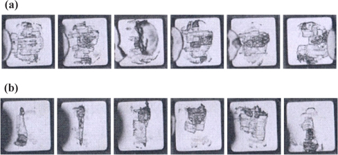
The BST was performed on one good die and one weaklybonded die, each contains multiple wire bonding pads, followed by JEDEC’s JESD22-B116, and the microscopic images of the bonding pads under the test are presented in Fig. 2. Ball detached footprints on the good dies showed a larger ball forming footprint on pads, as shown in Fig. 2(a). Smaller ball footprints with even line-shaped detachment in the direction of the BST were observed on the weakly-bonded die as shown in Fig. 2(b). Both well and weakly-bonded dies presented no of bond shear, bonding surface failure, shearing skip, or pad lift. The results showed no suspicious gold wire defects. Based on the ball size comparison and BST result, the surface condition of the aluminum pad was suspected to be the primary reason for the weaklybonded wire. This preliminary result matches with the visual inspection of the ball size presented in Fig. 1. Besides the BST, the ball pull test (BPT) was also performed on the two groups of samples. The BPT is one of the time-zero tests for wire bond strength and quality that uses tensile strength rather than the shear loading test in the BST. It has been suggested as an alternative to the BST for evaluating the solder joint integrity of area array packages [7]. It consists of applying an upward force under the wire to be tested, and it measures the pulling force at which the wire or bond fails in a grams-force metrics. Failure modes are the followings: (1) ball bond lifting; (2) neck break; (3) mid-span wire break; (4) heel break; and 5) wedge bond lifting. Similar to the BST, the test vehicle for the BPT was chosen from one good die and one weakly-bonded die. The test result were 7.9749 g-f and 0.4422 g-f for their mean and standard deviation, respectively. The BPT did not show any statistical significance based on a t-test of the two types of dies, but the previous BST result was enough to lead to an in-depth surface analysis of the aluminum bonding pads. An earlier study reported ball shearing and cratering caused from the formation of gold-aluminum intermetallic compounds with aging [8]; however, no evidence of the formation of intermetallic compounds on the pad surface was found in this study.
Two types of sample: good dies, from a wafer containing good wire-bonded dies, and suspicious dies, from a wafer containing weakly or poor wire-bonded dies, were selected for surface analysis using XPS, AES, and EDX. The detailed bonding-pad surface analysis is presented in the next section.
3.1 X-ray photoelectron spectroscopy (XPS)
X-ray photoelectron spectroscopy (XPS) is a quantitative spectroscopic measurement technique that measures the elemental composition, chemical state, and/or electron state of elements that reside on a material surface. The binding energy information of elements on a metal surface can be obtained from the shift in the binding energy of a core level electron and associated changes, such as multiple splitting and shake-up satellites, this presents the chemical status shift with the degree of electron bond polarization between nearest neighboring atoms. The XPS measurements were carried out on ESCALAB 210, manufactured by VG Science, with Mg-Kα excitation (hv=1,253.6 eV), and the peak-shaping for selecting binding energy was done using XPSPEAK 41.
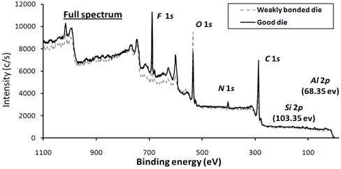
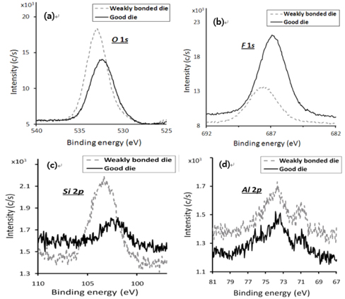
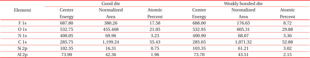
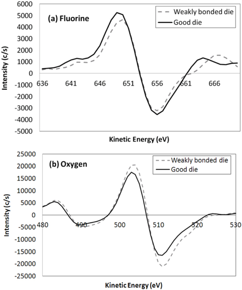
Acquired XPS data from the samples enhanced energy peaks of detected elements by aluminum source excitation were calibrated with the content of carbon, and the full XPS spectra are shown in Fig. 3. Detected elements are mostly fluorine, oxygen, carbon, and nitrogen, there are relatively small peaks of Si 2p and Al 2p. Comparing the two sample dies, the intensity of oxygen is increased for the weakly bonded die, this shows the natural surface passivation of Al2O3 and/or Al(OH)x (aluminum hydroxide) layer is increased. When we started our analysis we did not expect to find fluorine on the bonding pads, we conclude the fluorine we detected must have came from the plasma etching of the SiO2 passivation layer for the bonding pad opening process. Silicon oxide etching generally uses fluorine- containing gas species, such as CHF3, CF4, and C4F8, with augmented plasma enhancing gas species for a faster, more uniform etch. Fluorine contaminants released as an F residual on aluminum bonding pads can form AlF3 near the metal grain boundaries, and it can provoke the formation of Al(OH)3 crystals instead of the native thin Al2O3 layer growth. With some humidity, the formation of Al(OH)3 can be accelerated, leaving hydrofluoric acid (HF) on the aluminum bonding pads: AlF3 + 3H2O → Al(OH)3 + 3HF (↑). Figures 4(a)~(d) is the XPS spectra of the individual elements detected. Both good dies and weakly bonded dies are exposed to the same pad opening recipe with fluorine-containing plasma. We assume the same amount of fluorine was absorbed into the metal pads, but the decreased intensity of fluorine in Figure 4 (a) supports the possibility of the increased Al(OH)3 in the weakly bonded dies. Increased oxygen contents and no change in the intensity of aluminum, as shown in Figs. 4(b) and 4(c) match with our postulation of Al(OH)3 formation due to the absorption of fluorine by the aluminum. One might suspect the existence of an SiO2 residue from the increased Si 2p and O 1s seen in Figs. 4(b) and 4(d), but the intensity level was not significantly different from the other two samples to determine that the residue of SiO2 is responsible for this result. Our XPS analysis still remains so there is more room to reveal the processes at work, but similar work was suggested by Physical Electronics, a division of ULVAC-PHI [9].
3.2 Auger electron spectroscopy (AES)
To avoid any possible misleading data from the XPS analysis, Auger electron spectroscopy (AES) was also performed on the same types of sample. AES is a surface-specific analytical technique that utilizes a high-energy electron beam as an excitation source. Elements on the aluminum pads’ surface are excited by the electron beam and are relaxed under “Auger” electron emission. In our AES measurement, a neutral beam with Ar was used for beam generation, employing the PHI 700, manufactured by Physical Electronics.
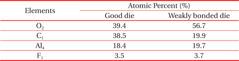
The weakly bonded die has a 44% larger atomic percentage in oxygen than that of a good die, and this result is in accord with the XPS analysis in Table 1 and 2. The atomic percentage of fluorine has only a 2% difference for the two samples, and this result does not clearly match with the previous XPS measurements. We think that the relatively smaller value of the fluorine count compared with the oxygen taken from the sample can dilute the trace existence of aluminum oxide compounds formed on the percentage value of fluorine, and the evidence of larger counts of oxygen certainly explain the formation of Al(OH)x as a hindrance to wire-bonding. Full spectra of AES measurements and selected fluorine and oxygen spectra are also provided in Figs. 5 and 6 for further investigation. Even though we used a weakly-bonded die, it is still not clear whether it is in the form of a thin film or crystallized by XPS and AES. In fact, there are a number of aluminum oxides, such as Al2O3 (oxide), AlOFx, AlO(OH)x (oxyhydroxide) and Al(OH)x (hydroxide) crystal structures.
[Table 1.] Periodic table of elements.

Periodic table of elements.
[Table 2.] AES Atomic percentage measurement.
AES Atomic percentage measurement.
3.3 Energy dispersive X-ray spectroscopy (EDX)
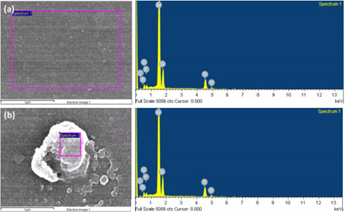
Microscopic surface morphology with elemental analysis was carried out by employing energy dispersive X-ray spectroscopy (EDX). EDX with a scanning electron microscope (SEM) provides a visualized surface morphology and specifies the chemical composition analysis. We measured two different, clean locations for each type of die, and their EDX profiles were similar for each measurement. High aluminum content was observed with no significant amounts of oxygen and fluorine, this infers no significant oxide compound was formed in the observed area. Figures 7 shows SEM images and EDX profiles acquired from (a) the clean area in the good die and (b) the contaminated spot in the weakly-bonded die, respectively. Observed contaminated spots showed a good increase of carbon and oxygen with much less aluminum content, the numerical measurements are presented in Table 3.
[Table 3.] Numerical analysis of EDX measurements.
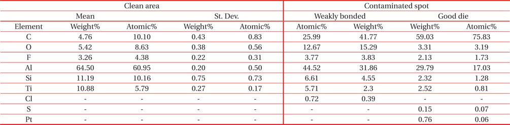
Numerical analysis of EDX measurements.
Observation of fluorine and increased carbon content can be explained by the plasma process for pad opening. The dry etch chemistry for the removal of the final oxide or nitride passivation layer before wire bonding and/or solder ball joining contains mostly fluorine species, such as CHF3, CF4, and C2F8. Fluorine radicals (F*) dissociated by applied RF power in plasma react with SiO2 to make a volatile product of SiF. Radicals are intermediates with an unpaired electron, and they are highly reactive with a shorter life cycle. RF plasma driven fluorine radicals have enough energy to be absorbed into the metal grain boundaries and form AlFx.
Once the pad opening process is complete in back-end manufacturing, wafers are packaged and shipped to back-end packaging manufacturing for the next operation. Sometimes the processed wafers can be stored in a container for a prolonged time. Depending on the processing and storing environment, fluorinated aluminum can form AlOFx, and Al(OH)x. Although the effect of fluorine maybe shown to be trivial in the EDX results, out postulation on the observed fluorine in the XPS analysis is still holds. The oxygen weight % increase from 5.70 to 12.67 may simply be explained by the oxygen supplied by humidity that reacted with aluminum, forming Al(OH)x crystal on the aluminum pad.
Ar plasma exposure for compound products cleaned by sputtering might help to remove AlOFx and Al(OH)x [10], but the high physical energies used can drive fluorine atoms to deeper region of the aluminum pad to cause weaker shear bonding. Surface treatment with atmospheric plasma before bonding can help to clean the surface while removing organic by-products [11], but this can also change the surface energy of the material causing lowered solder wettability. Although a number of US patents for the reduction of fluorine contaminants or defluoridation of metal have been claimed in the last few decades, no single best solution for this fluorine contamination has been proposed yet.
In addition to the fluorinated contaminants, chlorinated contaminants also need our attention. The aluminum pad is also patterned with chlorine containing plasma, such as BCl3 and CCl4. AlCl3, etch by-product is highly corrosive to the remaining aluminum film, and it can also provoke Al(OH)3: AlCl3 + 3H2O → Al(OH)3 + 3HCl. Chlorinated contamination on the bonding pad is much less likely than fluorinated contamination. Native oxide or aluminum hydroxide can be reduced by argon plasma sputtering or hydrogen plasma treatment.
In terms of the back-end fabrication process, using a photoresist strip after oxide pad opening is another consideration. Oxygen plasma ashing is the most commonly used method for photoresist stripping in manufacturing, and it can also be followed by a solvent strip. Once the fluorine contaminants reside on or between the grain boundary of the aluminum, it may form Al(OH)x or AlOFx.
The quality of the semiconductor device is not only defined by the performance, but also by their long term reliability. Quality control passed semiconductor packages that bear even one weakly bonded die due to surface contamination, can jeopardize the product’s reliability. We measured the surface conditions of two types of die, measured by XPS, AES, and EDX, and traced the evidence of fluorinated contamination and the formation of Al(OH)x and/or AlOFx through extensive surface analysis. In this paper, possible contamination sources of the aluminum bonding pad, from the previous plasma etching process for pad opening, were discussed. This work is limited to aluminum bonding pads, but the approach for solving this engineering problem still holds for copper interconnection. One possible suggestion to alleviate this concern is to use hydrogen plasma for surface treatment as well as PR ashing, but this is not mature technology yet. Hydrogen plasma photoresist ashing can also be beneficial for copper and low-k interconnections, this is currently under investigation with an augmented plasma process diagnosis using optical emission spectroscopy.