Photovoltaic ribbon is widely used as an electric wire to form a connection between Si solar cells in a module [1,2]. Conventional lead-containing solders (Sn-Pb) for photovoltaic ribbon have been widely used as low temperature joining alloys because of their good combination of process attributes, convenient material properties, and low cost [3-6]. The Sn-Pb solder is well known to have the eutectic composition of Sn62-Pb38 (wt%), and the eutectic temperature of 183℃ [7-10]. On the other hand, low melting Sn-Bi solder was recently shown to have the eutectic composition of Sn43-Bi57 (wt%) and the eutectic temperature of 139℃, which is very low [11-13]. Research about lowering the melting temperature of solder is required in the process of solar tabbing. This article presents a method for lowering the melting temperature of eutectic Sn62-Pb38 (wt%) solder by the addition of a small amount of Bi atoms.
The phase transformation of Sn-Pb-Bi solder for photovoltaic ribbon during soldering was studied using real-time synchrotron X-ray scattering. Synchrotron X-ray scattering with very high flux and high resolution is one of the best probes to examine the in-situ phase transformation of advanced materials [14,15]. The useful result was obtained, that the solder's melting temperature decreased from 183℃ to 170℃ by addition of a small amount of Bi atoms to the eutectic Sn62-Pb38 (wt%) solder.
Photovoltaic ribbons were made through melting plating with eutectic Sn62-Pb38 (wt%) solder, to which 0, 1, 2, 3, or 6 wt% of Bi was added, respectively. First, the Sn62-Pb38 (wt%) billet was melted using a melting plating pot at the temperature of 300℃. Next, Bi granules were added and mixed into the molten state, then the temperature was maintained after cooling to 250℃. The surface of copper ribbon was flux coated, and each of the photovoltaic ribbons were made by vertically dipping at the speed of 3.5 mm/sec into the melting plating pot.
Synchrotron X-ray scattering experiments were performed with the beamline 5D (GIST) at Pohang Light Source (PLS) in the Republic of Korea. The incident X-rays were vertically focused by a mirror, and monochromatized to the wavelength of 1.240 Å by a double bounce Si(111) monochromator. The experiment was carried out by measuring the conventional X-ray powder diffraction profiles at several temperatures during real-time annealing in air.
The surface and cross-section morphology of the photovoltaic ribbons was observed by using a scanning electron microscope (SEM). Each of the ribbons was fixed in a self-made sample holder for SEM analysis. Since Sn-Pb-Bi solder is very soft, the cross-section of the SEM samples was precisely polished. The peel strength between the photovoltaic ribbon plated with Sn- Pb-Bi solder and silver plate was measured using a peel strength tester. Since peel strength generally rises with the solder's thickness, the thickness of the Sn-Pb-Bi solder was measured from the cross-section of the ribbon on the SEM micrograph, and revised. Lastly, hardness of the Sn-Pb-Bi solder at the surface was measured using a Vickers hardness tester.
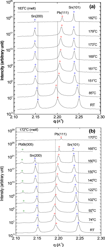
Phase transformation of the Sn-Pb-Bi solder during real-time soldering was first analyzed. Figure 1(a) shows the X-ray powder diffraction profiles of eutectic Sn62-Pb38-Bi0 (wt%) solder, measured at several temperatures with real-time synchrotron X-ray scattering during soldering, in air. At room temperature (RT), the Sn and Pb crystal phases were observed, as demonstrated by the Bragg reflections at qz= 2.155, qz= 2.201, and qz= 2.250 Å-1, which correspond to the crystalline Sn(200), Pb(111), and Sn(101) reflections, respectively [JCPDS 04-0673, JCPDS 04-0686]. The Sn and Pb crystal phases began melting at 182℃. The solder sample was observed to melt at 183℃, which is consistent with the eutectic temperature of 183℃ [7-9].
Figure 1(b) shows the X-ray powder diffraction profiles of the Sn62-Pb38-Bi3 (wt%) solder, measured at several temperatures during real-time soldering in air. At RT, the three reflections for Sn and Pb crystal phases were observed, as was seen in the Sn62- Pb38-Bi0 sample. By heating to 92℃, a new PbBi alloy crystal phase was formed, as demonstrated by the Bragg reflection at qz= 2.094 Å-1, which correspond to the crystalline PbBi(005) reflection [JCPDS 26-0215]. The PbBi had a large-sized, simple tetragonal crystal structure (a=9.93 Å, c=14.99 Å). The PbBi alloy phase grew further to 160℃, and began melting at 165℃. These results indicated that Bi atoms formed a PbBi alloy phase with some parts of the Pb, while an alloy phase with Sn atoms was not formed. In general, as the temperature increases, positions of diffraction peaks shift to the left due to thermal expansion of the solder. This was observed for the peak position of Sn(101) crystal phase, while that of the Pb(111) crystal phase was shifted to the right at temperatures above 102℃. The behavior of the Sn(101) and Sn(200) peak positions was similar, so the behavior of the Sn(101) peak was selected for analysis because its relative intensity was 100. This result was caused by the extraction of the Sn atoms in the Pb crystal phase. At the temperature of 160℃, the peak intensity of the Sn crystal phase first started to decrease. At 165℃, the peaks of the Sn crystal phase mostly disappeared, while the peak intensity of the Pb crystal phase also started to decrease. The solder sample was observed not to melt at 165℃, but at 170℃. The eutectic Sn62-Pb38 (wt%) solder is well known to have the eutectic temperature of 183℃ [7-9]; however, the useful result was observed that the solder's melting temperature decreased from 183℃ to 170℃ by the addition of a small amount of Bi atoms to the Sn62-Pb38 (wt%) solder.
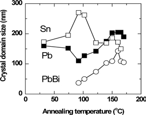
To illustrate the phase transformation quantitatively, the crystal domain sizes of the Sn(101), Pb(111), PbBi(005) Bragg reflections were plotted as a function of the annealing temperature. Figure 2 shows the evolution of the defect-free crystal domain sizes of the Sn, Pb, and PbBi crystal phases in the surface-normal direction during real-time annealing. They were estimated from the full-width at half-maximums (FWHMs) of the Bragg reflections using the Scherrer formula [16]. The crystal domain size of the Sn phase increased from 173 nm at RT to 270 nm at 92℃, then decreased to 150 nm as the temperature increased to 165℃. At the temperature of 165℃, the Sn crystal phase mostly melted. In the case of the Pb phase, the crystal domain size decreased from 160 nm at RT to 110 nm at 92℃, then increased to 205 nm as the temperature increased to 165℃. At the temperature of 170℃, the Pb crystal phase mostly melted. The PbBi alloy phase nucleated at 92℃, then grew further from 37 to 143 nm as the temperature increased to 160℃.
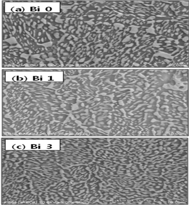
In order to observe the micro-morphology of the Sn-Pb-Bi solder, additional SEM experiments were conducted. Figure 3 shows the surface SEM micrographs of Sn62-Pb38-Bi (wt%) solders, according to the Bi composition. In the representation of the surface morphology of eutectic Sn62-Pb38 (wt%) solder without Bi, the brighter area shows the Pb crystal phases, which are surrounded by the darker area of the Sn crystal phases, as shown in Fig. 3(a). This result indicated that the Sn and Pb crystal phases existed separately, which is consistent with the results of synchrotron X-ray scattering. As the amount of Bi atoms increased from 1 to 6 wt%, as illustrated in Fig. 3(b) and 3(c), the mean size of the Pb crystal phase uniformly decreased, compared to the result without Bi atoms.
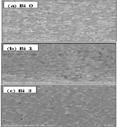
In order to observe the internal morphology of the Sn-Pb- Bi solder, cross-section SEM micrographs of the solders were made. Figure 4 shows the cross-section SEM micrographs of Sn62-Pb38-Bi (wt%) solders, according to Bi composition. In the internal morphology of eutectic Sn62-Pb38 (wt%) solder without Bi, the Pb crystal phases are surrounded by the Sn crystal phases, as shown in Fig. 4(a). The mean size of the Pb crystal phase decreased as the amount of Bi atoms increased, as illustrated in Fig. 4(b) and 4(c), which is also consistent with the results of the surface morphology.
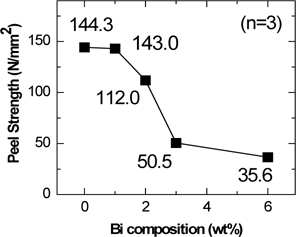
The peel strength between the solar cell and the ribbon is important for providing a long lifespan to the photovoltaic module. Figure 5 shows the peel strength of Sn62-Pb38-Bi (wt%) solder, according to Bi composition. Peel strength decreased with an increasing composition of Bi atoms in the solders. When the amount of Bi atoms was 1 wt%, the peel strength was similar to that of the eutectic Sn62-Pb38 (wt%) solder without Bi, while the peel strength largely decreased when the amount of Bi atoms went over 2 wt%. Considering these results, addition of 1 wt% of Bi atoms to the eutectic solder would be an appropriate composition to maintain the long lifespan of the photovoltaic module.
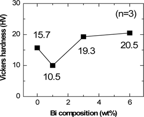
To provide photovoltaic modules at a low price, decrease in the thickness of the silicone solar cell is required [17,18]. Therefore, photovoltaic ribbon requires a decrease of copper’s yield strength and the hardness of the solder in order to promote a safe tabbing process. Figure 6 shows the Vickers hardness of Sn62-Pb38-Bi (wt%) solder, according to Bi composition. When the amount of Bi atoms was 0 wt%, the hardness was 15.7 HV. The hardness decreased to 10.5 HV at 1 wt% Bi, but increased again to 19.3 HV when the amount exceeded 3 wt%. Considering these results, addition of 1 wt% of Bi atoms to the eutectic solder would be an appropriate composition to promote a safe tabbing process.
We studied the phase transformation of low melting Sn62- Pb38-Bi3 (wt%) solder for photovoltaic ribbon during soldering by using real-time synchrotron X-ray scattering. At RT, the Sn and Pb crystal phases in the solder existed separately. By heating to 92℃, a new PbBi alloy crystal phase was formed, while the Sn and Pb crystal phase already existed. The PbBi alloy phase grew further to 160℃. These results indicated that Bi atoms formed a PbBi alloy phase with some parts of Pb, but not with Sn atoms. The extraction of Sn atoms in the Pb crystal phase at temperatures above 102℃ was also observed. The Sn crystal phase first began melting at 160℃, and was mostly melted at 165℃. In contrast, the Pb and PbBi crystal phases started to melt later, at 165℃, and were mostly melted at 170℃. The useful result was observed, that the solder's melting temperature decreased from 183℃ to 170℃ by adding a small amount of Bi atoms to the eutectic Sn62-Pb38 (wt%) solder. Our study first revealed the detailed in-situ phase transformation of the Sn-Pb-Bi solder during heating up to the eutectic temperature. Considering the results of peel strength and hardness, adding 1 wt% of Bi atoms to the eutectic Sn62-Pb38 (wt%) solder would be an appropriate composition to promote the formation of good properties.