Recently, smooth sidewalls in trenches, and round corners at the via bottom are required for device isolation, the formation of vertical capacitors in integrated circuits, and waveguides in optoelectronics and microelectro-mechanical systems. Smoother sidewalls in the trench and round corners at the via bottom prevent voids during trench refilling, and avoid breakdown of the dielectric film covering the trench sidewalls, and while round corners reduce the build-up of mechanical stress onto a silicon surface [1-9].
Until now, the dimensional reactive and etch characteristics of silicon during reactive ion etching (RIE) in the inductively coupled plasma (ICP) have not been completely uncovered. The ICP source shows the characteristics of a high etch rate, and it is used for high aspect ratio structure applications. Some of the basic properties and the process performance, were previously reported [11-15]. However, the purpose of this study is to minimize the loading effect in deep trench silicon etching and ensure the bottom profile, by using ICP. So the etch rate was measured as functions of the various etching parameters, and this is needed to enhance the etch selectivity and uniformity, and to eliminate the pressure effect with the anisotropic profile.
In this work, the etching of silicon in SF6/O2 plasma at different O2 content is considered, using the ICP. The etch characteristics of the silicon were investigated, in terms of the etch rate and the selectivity. At the same time, the etch rate was measured as functions of the various etching parameters (gas mixing ratio, RF power, and process pressure). For elemental analysis of the surface of the etched silicon, field emission-auger electron spectroscopy (FE-AES) was used, and this technique is known to be surface-sensitive. The chemical binding states on the surface of the etched silicon were investigated by x-ray photoelectron spectroscopy (XPS). Field emission-scanning electron microscopy (FE-SEM) was used, to investigate the etch profile.
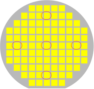
The substrate was 6-in p-type Si (100), and its resistivity was in the range of 5~30 ohm·cm. The etching experiments were performed in an ICP system (Multiplex ICP, STS Co.). The SiO2 thin film was measured by a surface profiler (KLA Tencor, α-step 500) and FE-SEM (Sirion 400, FEI), before the etching experiments. As shown in Fig. 1, the selected positions in the Si substrate were analyzed, by measuring the etch rate, selectivity, and uniformity. The etch characteristics of the Si films were investigated as a function of the SF6/O2 gas mixing ratio. In addition, the etching of the Si films was investigated by changing the etching parameters. The etch rate of all point areas was measured by a surface profiler (KLA Tencor, α-step 500) and FESEM (Sirion 400, FEI). The compositional changes on the surface of the etched Si films were investigated, using XPS (SIGMA PROBE, Thermo VG Scientific). The spectra were plotted, by counting the photo electrons at kinetic energy intervals of 0.1 eV. The detailed information on the inner region of the film was provided by the spectra recorded at the electron take-off angles of 90°. The FE-AES (Microlab 310-D, Thermo VG Scientific) technique used for the elemental analysis on the surface of the etched Si films is a surface-sensitive spectroscopic technique, and all of the samples for the XPS and FE-AES analysis were bare Si films that did not have any photoresist patterns at the time of etching. The size of the samples was 6-in Si (100), and the etching time was 60 sec. The etching profile of the crosssection was characterized, using FE-SEM. The Si films used for measuring the etch rate and etching profile had a photoresist pattern (SS03A9). The width and thickness of the PR pattern were 1.5 and 1.02 ㎛, respectively.
For the etch characterization of the Si film in the ICP system, the etch characteristics of the Si film were systematically investigated as a function of the SF6/O2 gas mixing ratio, RF power, and process pressure. Generally, the combination of SF6 and O2 enhances the etch rate of the silicon, by forming volatile etch byproducts, such as SiFx and O-fluorides. Otherwise, it decreases the etch rate, by forming non-volatile etch by-products of F-Si or O. If F-Si or O is accumulated on the surface, this layer precludes any chemical reactions between F and Si [16,17].
3.1 The effect of the etch characterization in the ICP system
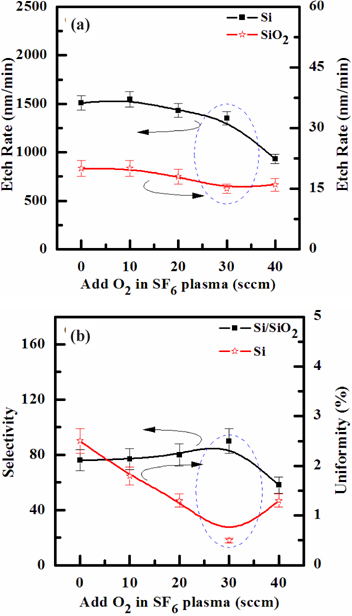
Figures 2(a) and (b) show the etch rate and selectivity of the Si film as a function of the SF6/O2 gas mixing ratio, respectively, when the total flow rate was fixed at 160 sccm. The other process conditions, viz. the RF power, platen power, process pressure, and substrate temperature, were maintained at 600 W, 20 W, 94 mTorr and 45℃, respectively. As the O2 content in the SF6/O2 gas plasma increased from 0 to 40 sccm, the etch rates of the Si films decreased from 1,510 to 943.4 nm/min. But, when the O2 content increased over 30 sccm, the selectivity of Si to SiO2 increased. As the O2 content in the SF6/O2 plasma increased from 0 to 30 sccm, the etch uniformity of Si films decreased from 2.5 to 0.5. The optimum etch rate, selectivity and uniformity of the Si film were 1,350 nm/min, 90, and 0.5%, at the O2 content of 30 sccm in the SF6 plasma. The comparisons on etch rates of the Si film in SF6-based plasma show that chemical etching is more effective than physical sputtering. It is well known that the fluorine component reacts with Si thin film, to form highly volatile by-products, such as SiF4 (melting point: - 90℃ and boiling point: - 86℃). The evident enhancement on etch rate of the Si film in the pure SF6 plasmas suggests that the chemical etch pathways provided by the F-atoms are the dominant mechanism for the given set of input process parameters. In the case of the physical sputtering of Si films, we expect that the contribution is much lower than from ion-assisted chemical reactions. In SF6-based plasma, increasing the O2 content up to 30 sccm decreases the etch rate via two different mechanisms: (1) decreased chemical reactions by the ion-stimulated desorption of the reaction products and (2) the decreased contribution of physical sputtering. Nevertheless, when the O2 content exceeds 30 sccm, the etch rate begins to decline, due to the interruption of physical sputtering. This implies that for a given range of experimental conditions, chemical reactions were more effective than the physical etch pathway [23,24].
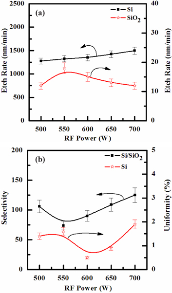
Figure 3(a) shows the effect of the RF power on the etch rates of Si film, in the SF6/O2 (=130:30 sccm) plasma. As the RF power applied to the ICP coil was raised from 500 to 700 W, the etch rate of the Si films increased from 1,277 to 1,497 nm/min. Figure 3(b) shows the selectivity change of Si to SiO2. When the RF power applied to the ICP coil was raised from 500 to 550 W, the selectivity decreased from 106 to 74; but when the RF power was raised from 550 to 700 W, the selectivity increased. Such behavior of etch rates with increasing input power may be explained by the acceleration of both the physical and chemical etch pathways, through the increasing volume densities and fluxes of ions and chlorine atoms [23].
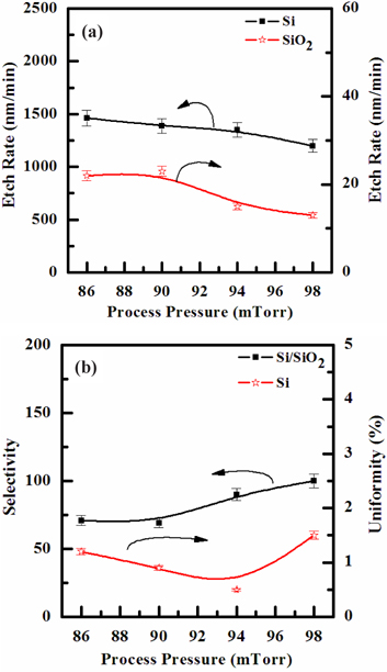
Figure 4(a) shows the etch rate of Si film, as a function of the process pressure, in the SF6/O2 (130:30 sccm) plasma. As the process pressures increased from 86 to 98 mTorr, the etch rates of the Si film decreased from 1,463 to 1,200 nm/min. The reduction in process pressure enhances the density of the chemically active neutral species, which accelerates the chemical reaction. However, since the mean free path is decreased, and the ions energy is increased with increasing the process pressure, the ion stimulated desorption of the reaction products is increased, and the fraction of free surface available for the chemical reaction is decreased. Similar to the effect of the gas mixing ratio discussed above, these two contrary factors produce the nonmonotonic behavior of the etch rate. Figure 4(b) shows that the selectivity of Si to SiO2 increased from 71 to 100, in the same condition in which the process pressure was raised from 86 to 98 mTorr,.
From the above results, we hypothesize that the molecular bonds were broken by the ion bombardment on the surface of the Si film. Frequent chemical reactions in the plasma were facilitated by the higher ion density, and the increased number of broken molecular bonds. This conclusion is in good agreement with the data shown from Fig. 2(a) to Fig. 4(b) [18-25].
For more detailed investigation of the chemical reaction on the etched surfaces of the Si films in plasma, as a function of SF6/O2 gas mixing ratio, XPS analysis was carried out. We compared the differences between the chemical reactions on the surface of the etched Si film, and on the surface of the as-deposited Si film. We also compared the differences between the peaks from the as-deposited Si film, and the etched Si films, in order to evaluate the changes of the chemical shift. The input plasma parameters were as follows: RF power of 600 W, platen power of 20 W, process pressure of 94 mTorr, and substrate temperature of 45℃.
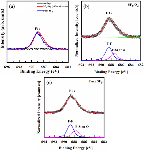
Figure 5 shows the high-resolution F 1s XPS spectra obtained from the surface of the Si film, before, and after, etching in the SF6/O2 (130:30 sccm) gas mixing ratio, with RF power of 600 W, platen power of 20 W, process pressure of 94 mTorr and substrate temperature of 45℃. No peak for the Si-Fx bond was detected in the XPS analysis, thus indicating that the Si fluoride is removed during the etching process. The reference F 1s peak is 688.2 eV. As shown in Figs. 5(b)~(c), the peak intensity of F 1s increased, and shifted to the higher energy. The F 1s peak of as-deposited Si film showed no peak. As shown in Fig. 5(b) SF6/O2 plasma and (c) pure SF6 plasma, the F 1s peak was deconvoluted into two peaks, which were deemed to correspond to the oxygen and hydroxyl group on the surface in the SF6/O2 and the pure SF6 plasma, respectively: the deconvoluted peak values were F-F bond (687.4 and 687.7 eV), and F-Si or O bond (686.1 and 686.4 eV). From these results, we could consider that the chemical etching mechanism of the Si film was changed by SF6 gas, and the chemical etch mechanism of the Si film was not changed by varying the gas ratio [31].
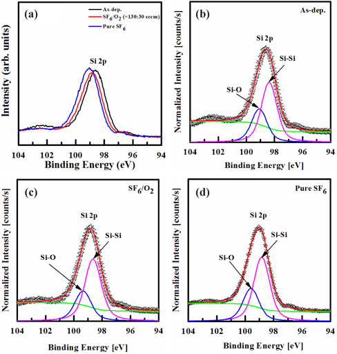
Figure 6 shows the XPS narrow-scan spectra for Si 2p, taken at a 90˚ angle. These spectra of the Si film surface were taken before, and after, etching in pure SF6 and SF6/O2 gas mixture. The peaks obtained from the as-deposited Si film were used as a reference. When the Si film was exposed to the SF6/O2 plasma, the core peak of Si 2p was shifted to the higher binding energy of 98.8±0.4 eV. Also, when the Si film was exposed to the pure SF6 plasma, the core peak of Si 2p was shifted to the higher binding energy of 99.1±0.6 eV. As shown in Fig. 6(a), a few chemical shifts occurred in the plasma, but the shape of the Si 2p peak was broadened. For the as-deposited film, as shown in Fig. 6(b), the Si 2p peak can be decomposed into two peaks, corresponding to the Si-Si bond (98.4 eV), and Si-O bond (99.1 eV). Compared to these, the deconvoluted peaks of the etched Si film in the SF6/O2 plasma (98.7 and 99.4 eV) and pure SF6 plasma (98.9 and 99.6 eV) show a noticeable shift in the Si 2p (98.4 eV) peaks, as shown in Figs. 5(c)~(d), which can be attributed to the destruction of the oxide bonds by ion bombardment. This chemical shift indicates that a chemical reaction occurred between Si and F, resulting in the formation of Si-F bonds on the surface [26].
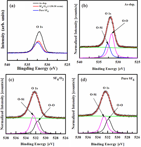
Figure 7 shows the XPS narrow-scan spectra for O 1s, taken at a 90˚ angle. These spectra of the Si film surface were taken before, and after, etching in pure SF6 and SF6/O2 gas mixture. The peaks obtained from the as-deposited Si film were used as a reference. The peak at 531.9 eV corresponds to the O 1s bond. As shown in Fig. 7(a), the chemical intensity was decreased in the etched sample in the plasma. For the as-deposited film, as shown in Fig. 7(b), the O 1s peak can be decomposed into two peaks, corresponding to the O-O (531.7 eV) and O-Si (532.8 eV) bonds. As shown in Figs. 7(c)~(d) for O 1s, after etching the Si film in the plasma, the decomposed O 1s peaks at 531.7 and 532.8 eV were decreased in intensity, and no shift was observed, as a result of the preferential removal of the adsorbed molecules. However, in the spectra of the Si films etched in the SF6/O2 and pure SF6 plasmas, the deconvoluted O 1s peak intensities, corresponding to the O-O and O-Si bonds, decreased, owing to the formation of O-F bonds. The XPS results reveal that Si, F, and O were removed by chemical reactions with F radicals, and by the ion bombardment [27-29].
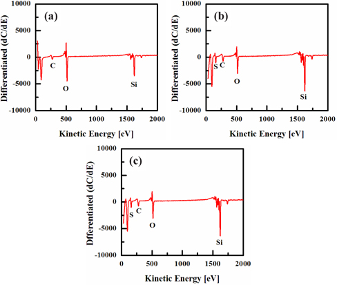
Figure 8 shows the composition on the surface of the Si film obtained by FE-AES analysis, as a function of the SF6/O2 gas mix ratio. The input plasma parameters were as follows: RF power of 600 W, platen power of 20 W, process pressure of 94 mTorr, and temperature of 45℃. The presence of silicon was confirmed by FE-AES analysis, as shown in Fig. 8. The results of this analysis are associated with the efficiency of the ion-stimulated desorption of the reaction products. The etching time was 60 sec. The surfaces of all the samples were contaminated with carbon and oxygen, owing to their exposure to air, as shown in Fig. 8. The F elements were not detected in the fluorine coating before, and after, etching in the plasma by FE-AES analysis, which may be due to the low contents of F on the surface. The existence of the F element in the FE-AES analysis was confirmed by the detection of silicon fluorine in the XPS analysis [31].
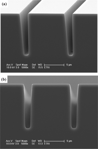
Figure 9 shows the side and cross-sectional SEM images of the Si film, after 4 min etching in SF6/O2 (130:30 sccm) plasma, at a fixed RF power of 600 W, platen power 20 W, process pressure of 94 mTorr, and substrate temperature of 45℃. After the etching of the Si films, the surface polymers were removed by standard cleaning (H2SO4+H2O2=4:1 cleaning, 100:1 HF= 120 sec, and spin rinse dry processing), and the removal step for the silicon dioxide mask was carried out to obtain a good profile for the silicon etching. As shown in Fig. 9, a high ratio vertical etching profile was observed after plasma etching of the Si film, due to the high etch rate of the Si film associated with F-radicals in the gas mixture.
We investigated the etch characteristics of Si film, using an ICP system. The etch characteristics were investigated, measuring the etch rates of the Si film with varying etch parameters. The optimum etch rate, selectivity, and uniformity of the Si film were 1,350 nm/min, 90, and 0.5%, respectively, at the O2 content of 30 sccm in the SF6 plasma. As the fraction of O2 in the SF6/O2 plasma was increased from 0 to 30 sccm, the etch rate of the Si film decreased. But, the selectivity and uniformity of the Si film increased with the further addition of O2 gas. Ion bombardment was required, due to the relatively high volatility of the by-products formed during etching by the SF6/O2 plasma. The chemical states on the surface of the etched Si films were investigated, using XPS. The etch mechanism of the Si film can be explained as follows: Si interacted with the F-radicals in the SF6 containing plasma, but remained at the surface, due to the high volatility of SiFx, which can be effectively removed, with the help of ion bombardment. This tendency agreed well with the general energy dependency of the ion-enhanced chemical etching yields.