With the feature size of conventional floating gate type nonvolatile semiconductor memory (NVSM) approaching to its scaling limitation, tremendous effort has been made to explore lowcost, high-density, and nonvolatile solid state memory devices, for use in mobile electronics, such as digital cameras, mobile phones, and MP3 players [1]. Based on the concept that charges are stored in discrete traps within the charge trapping layer, polysilicon-oxide-nitride-oxide-silicon (SONOS) charge trapping flash memories with nitride (Si3N4) [2] as the charge trapping layer has attracted much attention, for commercial applications to replace the conventional FG-NVSM. However, using Si3N4 charge trapping layer in a SONOS structure leads to poor retention, due to the shallow traps, and the small conduction band offset at the Si3N4/tunneling layer interface [3]. Employing high-k dielectrics as the charge trapping layer to improve memory characteristics in SONOS structure has been reported by many researchers [4- 9]. The high-k charge trapping layer allows a higher electric field cross the tunneling layer, due to electric flux density continuity [3], and results in a modified Fowler-Nordheim tunneling, due to the smaller conduction band offset (CBO) with a Si substrate [10]. However, pure high-k dielectrics as charge trapping layer, such as HfO2 and ZrO2, have poor retention characteristics, due to the presence of conduction paths in the high-k material [11]. In this paper, we report the improved memory characteristics, by NH3 annealing ZrO2 based charge trapping memory.
The P-type Si (100) substrates were cleaned by the standard Radio Corporation of America (RCA) process to remove native oxide. Then, a 4 nm SiO2 was thermally grown in dry O2 at 900℃, as the tunneling layer (TL). After that, the ZrO2 charge trapping layer (CTL) with a thickness of ~6 nm was deposited by pulse laser deposition (PLD), at a substrate temperature of 350℃ (a KrF excimer laser operating at 1-5 Hz was used for ablation; the laser fluence was around 1.8 J/cm-2; the deposition was performed under oxygen pressure of 1×10⁻⁴ Pa, and the growth rate per laser shot was approximately 0.1 nm). Subsequently, a ~8 nm Al2O3 film as blocking layer (BL) was deposited by atomic layer deposition (ALD), using tri-methylaluminium (Al(CH3)3) precursors, at a substrate temperature of 300℃. During this process, O3 was used as oxygen source. The fabricated memory capacitor without post-annealing is denoted as Z1. After the above processes, the memory capacitors were rapid thermal annealed (RTA) at 900℃ for 60s in N2 and NH3 atmosphere, denoted as Z2 and Z3, respectively. Finally, platinum (Pt) top electrodes with an area of cm2 were deposited on the films, by using magnetron sputtering technique, at room temperature. Ag silver paste was spread on the back side of Si substrate, as the bottom electrodes. The interfacial structure of the memory capacitors was revealed by crosssectional high-resolution transmission electron microscopy (HRTEM) images. To prepare the cross sectional sample of the memory structure for HRTEM, a standard technique was used, which including gluing two deposited structures, cutting, grinding, polishing, and thinning, via room temperature argon milling procedures. X-ray diffraction (XRD) was employed, to investigate the crystalline structure of ZrO2 films. The electrical characteristics of the memory capacitors were measured using a Keithely 4200 semiconductor characterization system (4200 SCS), in dc sweeping mode and pulse mode.
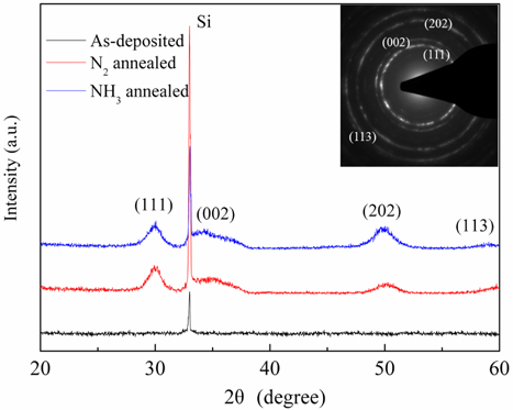
The XRD patterns of as-deposited and annealed ZrO2 films are presented in Fig. 1. It is observed that as-deposited ZrO2 films remain amorphous, while some crystalline peaks appeared after RTA at 900℃ in N2 and NH3 atmosphere, and the diffraction peaks are of tetragonal ZrO2 phase. The selected area electron diffraction (SAED) pattern of the NH3 annealed ZrO2 film is shown in the inset of Fig. 1. The Polycrystalline diffraction rings correspond to the (111), (002), (202) and (113) planes of the tetragonal ZrO2 phase, respectively.
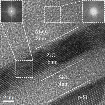
The cross-section and interface quality of the NH3 annealed memory capacitor was examined by HRTEM, as shown in Fig. 2. It can be seen that the thicknesses of TL, CTL and BL are 4 nm, 6 nm and 8 nm, respectively, and the interfaces are clear. The insets exhibit fast Fourier transform (FFT) analyses of selected areas, which reveal the crystallization characteristics. It is observed that the ZrO2 charge trapping layer crystallizes, after postannealing treatment. Meanwhile, Al2O3 films as blocking oxide still keep their amorphous structure.
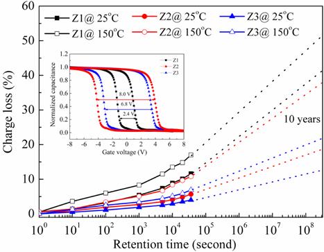
Figure 3 illustrates the data retention characteristics of memory capacitors at 25℃, and 150℃. The charge loss was 11.6%, 5.7% and 4% up to 4×10⁴s, for the three samples at 25℃, respectively. In order to predict the charge retention characteristics for a long time, according to the changing trend of the last three experimental data, we extrapolated the last two data, and supposed that the trend of charge loss fits a linear relation with the logarithm of retention time, up to ten years [6,9]. The extrapolation of the experimental results shows that the charge losses after ten years were 41.2%, 18% and 12.8%, respectively, suggesting that the NH3 and N2 annealing treatment could reduce the charge loss. The Z3 sample obtained optimum retention performance, which could be ascribed to the generation of deep level bulk charge traps, and reduced shallow level and interfacial traps in CTL [12]. These deep level traps are more immune to tunneling of electrons back to the substrate. For the three samples, it was observed that the charge losses after ten years at 150℃ can be determined to be 52.3%, 37.5% and 22.3%, respectively, by extrapolating the experimentally measured charge loss curve. It is well know that the charge loss mechanisms are composed of two categories. The first one, including electrons tunneling from trap to band, electron trap to trap tunneling, and holes band to trap tunneling, is not temperature sensitive. The second category, coming from thermal excitation, is temperature dependent. Trap to band tunneling and thermal excitation are the dominant charge loss mechanisms, and jointly contribute to charge loss for memory devices [13-16]. In our case, the charge loss increased with increase of temperature resulting from thermal excitation, and more electrons were discharged via thermal excitation into the conduction band of the charge trapping layer, then tunneled back to the silicon substrate. The best retention characteristics of the Z3 sample at 150℃ should be attributed to the generated deep level bulk traps, which could effectively resist the thermal excitation. The inset shows high frequency (1MHz) C-V hysteresis memory windows of the memory capacitors, measured with identical sweeping gate voltage (±8 V). For the three samples, the hysteresis memory windows were measured to be 2.4 V, 6.8 V and 8.0 V, respectively. These results should be attributed to the increase of charge traps near the TL/ CTL interface, and bulk of CTL, after post annealing treatment. Compared with Z1 and Z3 samples, Z2 sample obtaining the largest memory window results, from generating more interfacial traps and oxygen vacancies between the TL/CTL interface [17]. Compared with N2 annealing, although NH3 annealing generates less traps, a lot of the traps are deep level bulk traps, which are the dominant factor of the retention characteristics, especially at high temperature.
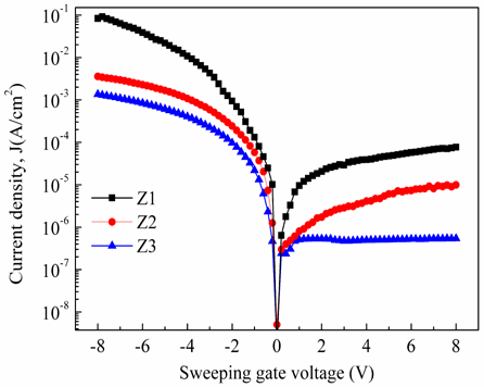
Figure 4 shows the leakage current density-voltage (J-V), for Z1, Z2 and Z3 samples. It is observed that the leakage current is lower for Z2 and Z3, compared to Z1, suggesting that the post annealing in NH3 or N2 atmosphere could effectively improve the interface quality, and reduce the interfacial defects of TL/CTL, since the undesired interface traps can be effectively suppressed, since the nitrogen bloked the atomic diffusion, and reduced the growth of the interfacial layer for Z3, by the NH3 annealing [18]. The results indicated that NH3 annealing treatment is a more effective method to improve the electrical performance, compared to N2 annealing.
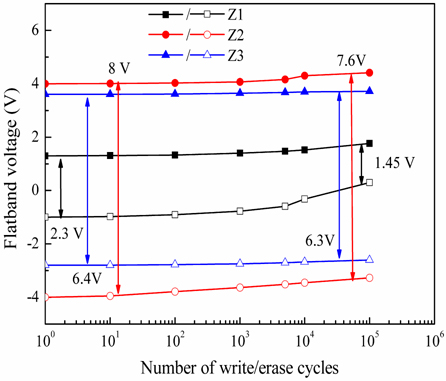
Figure 5 is the endurance performance of the three memory capacitors, and the program (solid symbols)/erase (open symbols) conditions were +8 V for 1 ms and -8 V for 1 ms, respectively. For the three memory capacitors, the memory window is degraded by 37%, 5% and 1.5% after 105 P/E cycles, respectively. For Z1 sample, the narrowest memory window resulted from the oxide traps and interface state generation at different locations depending on bias conditions, due to the memory structure being stressed for a long time [19]. On the other hand, the slight degradation of the memory window for Z2 and Z3 samples should be ascribed to producing stronger chemical bonds at the TL/CTL interface, and the interfacial quality and structure being improved after NH3 or N2 annealing treatment.
Pt/Al2O3/ZrO2/SiO2/Si memory capacitors have been prepared, and the effects of annealing atmosphere (N2 and NH3) on the memory characteristics have been investigated. It was found that the memory windows were improved, after annealing treatment. Excellent endurance and retention characteristics, even at 150℃, have been achieved, by using NH3 annealing. The results are attributed to deep level bulk charge traps, induced by using NH3 annealing. It looks like the NH3 annealed memory capacitor will be a potential candidate, in future nonvolatile flash memory device application.