Recently, the scaling down of SiO2 thickness has exacerbated problems such as increased leakage current, poly-Si gate depletion, and boron penetration into the channel region. Therefore, the still high-
In this work, we investigated the etch characteristics of the HfAlO3 thin films, using an inductively coupled plasma (ICP) system. The etching characteristics of the HfAlO3 thin film were investigated in terms of the selectivity of HfAlO3 to SiO2 as a function of added O2 gas in Cl-based gas chemistry. The chemical states on the surface of the etched HfAlO3 thin film were investigated by X-ray photoelectron spectroscopy (XPS). Auger electron spectroscopy (AES) was used for elemental analysis on the surfaces of the etched HfAlO3 thin film. Field emission-scanning electron microscopy (FE-SEM) was used to investigate the etch profile.
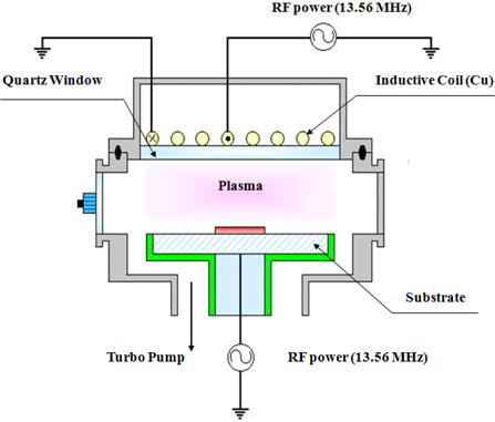
The HfAlO3 thin films were deposited on SiO2/Si 6-in p-type (100) wafers, by an atomic layer deposition (ALD) system. HfAlO3 thin film was deposited on the SiO2(100 nm)/Si(100) by ALD, with a thickness of 200 nm. The dry etching of the HfAlO3 thin films was performed, using an ICP system [10,11]. A 13.56 MHz power generator was connected to a 3.5 turn copper coil, to generate the ICP. Another 13.56 MHz power generator was attached to the substrate electrode, to control the DC-bias voltage. The substrate temperature was kept at 30℃, with a water-cooling system. The chamber was pumped to 10-4 Pa. The final pressure was lower than 10-4 Pa, using a turbo-molecular pump. The etching characteristics of the HfAlO3 thin films were investigated as functions of the O2/Cl2/Ar and the O2/BCl3/Ar gas mixing ratio. The etching conditions of the RF power, DC-bias voltage, and process pressure were 600 W, - 150 V, and 1 Pa, respectively. The etch rates were measured, using a surface profiler (Alpha-Step 500, KLA-Tencor). AES analyses were performed with a scanning auger microprobe (Microlab 350, VG Scientific). The composition change on the surface of the etched HfAlO3 thin film was analyzed by XPS. The XPS spectra were collected using a VG Scientific ESCALAB 250 instrument, equipped with an analytical chamber. The chamber was pumped down to a base pressure of less than 10-8 Pa with a twin-anode x-ray source, and a spherical sector analyzer with multichannel detectors. The samples were mounted on stainless steel stubs using double-sided adhesive tape, and Al
3.1 The effect of added O2 gas in the BCl3- and Cl2-based gas mixture
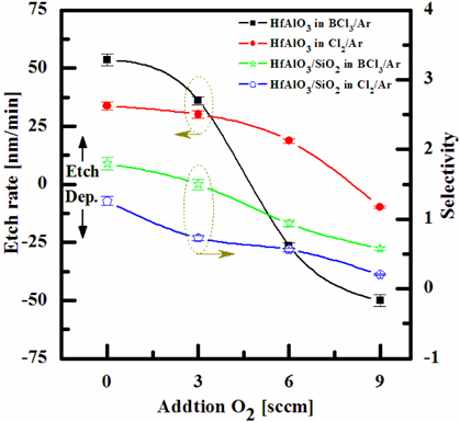
To evaluate the etch characteristics of the HfAlO3 thin films in an ICP etching system, the HfAlO3 thin films were etched by varying the BCl3/Ar and Cl2/Ar gas chemistry. The etch characteristics of the film in chlorine plasma need to be studied, when chlorine gas was used for the HfAlO3 thin film etching process. So, we investigated the etching characteristics of HfAlO3 thin film in BCl3- and Cl2- inductively coupled plasma. The O2 gas was added for passivation of the etching profile and the etch rate in the BCl3/Ar and Cl2/Ar mixing ratio [11]. Figure 2 shows the etch rate of HfAlO3 thin film, and the selectivity of HfAlO3 to SiO2 as a function of O2 content in the Cl2/Ar and BCl3/Ar gas mixture. The other conditions, of the RF power, DC-bias voltage, and process pressure, were kept at 600 W, - 150 V, and 1 Pa, respectively. The etch rate of the HfAlO3 thin film and the selectivity of the HfAlO3 to SiO2 were 36 nm/min and 1.5, and 30.1 nm/min and 0.73, in the O2/BCl3/Ar(=3:4:16) and O2/Cl2/Ar(=3:4:16) gas mixtures, respectively. As the O2 concentration increased from 0 to 9 sccm in the BCl3/Ar (=4:16) gas mixture, the etch rate of the HfAlO3 thin films and the selectivity of HfAlO3 to SiO2 decreased from 53.54 to -50.05 nm/min, respectively. As the O2 concentration increased from 0 to 9 sccm in the Cl2/Ar (=4:16) gas mixture, the etch rate of the HfAlO3 thin film decreased from 33.7 to -9.8 nm/min. In our opinion, the domination of the chemical reactions can be explained by the following factors. A) The melting points of HfCl4 and AlCl3 are about 432 and 192.6℃, and the domination of the chemical pathway may be related to its lack of volatility; by contrast, the melting points of the Hf-Cl4 and Al-Cl3 are lower than the melting point of Hf-Al-O (=up to 2,000℃). B) The Hf-Cl and Al-Cl chemical bonds (kJ/mol) have a lower Gibb’s free energy. The decrease of chemical bonds was due to the decreasing density of BCl or Cl radicals by reaction with O radicals, because the BCl and Cl atoms formed in the plasma spontaneously reacted with HfAlO3 [12,13].
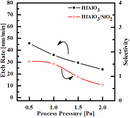
Figure 3 shows the etch rate of HfAlO3 thin film as a function of the process pressure, in the O2/BCl3/Ar(=3:4:16 sccm) plasma. As the process pressures increased from 0.5 to 2.0 Pa, the etch rates of HfAlO3 thin film decreased from 45.9 to 23.74 nm/min. The decrease of the process pressure enhances the density of the chemically neutral active species, which accelerates the chemical reaction [23]. However, since the mean free path and energy of the ions decrease with decreasing process pressure, the ion stimulated desorption of the reaction products is decreased, and the fraction of free surface available for the chemical reaction is increased. As a result of the pressure effect on the etch rate of the HfAlO3 thin film, the etch process is limited by the supply of the chemical source; and thus, the etch rate of HfAlO3 thin film decreases with decreasing process pressure [16].
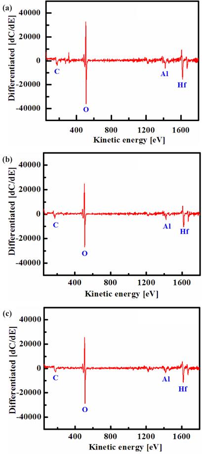
The samples were investigated by XPS and AES, to analyze the chemical states on the surface of the etched HfAlO3 thin films exposed to the O2/Cl2/Ar(=3:4:16 sccm) and O2/BCl3/Ar(=3:4:16 sccm) plasmas. The input plasma parameters were set to an RF power of 600 W, DC-bias voltage of - 150 V, process pressure of 1 Pa, and substrate temperature of 30℃. No boron peaks were detected. This means that the boron and chlorine compounds are highly volatile ones, such as boron-oxy-chloride (BOCl) or trichloro-boroxin (BOCl)3 [24].
Figure 4 shows the AES surface scan spectra of the HfAlO3 thin film for (a) the as-deposited films and the surface of the etched HfAlO3 thin films in (b) the O2/Cl2/Ar, and (c) O2/BCl3/Ar plasma, respectively. The etching time of the HfAlO3 thin film was 10 sec. Figure 4 (a) shows an AES surface scan of the as-deposited HfAlO3 thin film, in which O peaks are detected. The origin of carbon elements is the contamination in the etching chamber or the air. After etching, no B or Cl-related peaks were observed. With the addition of O2 gas, the intensity of Hf, Al and O peaks decreased, compared to that of the etched sample in BCl3/Ar and Cl2/Ar plasmas. This result means that by-products, such as Hf- Ox and Alx-Oy, increased on the etched surface in O2/BCl3/Ar and O2/Cl2/Ar plasmas. Therefore, the AES data clearly show that the surface of the etched HfAlO3 thin films in O2/BCl3/Ar and O2/Cl2/ Ar plasmas are formed with nonvolatile etch products, such as Hf-Ox, Alx-Oy, Hf-Clx, and Al-Clx .
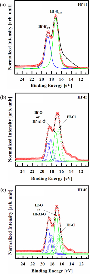
Figure 5 shows the deconvoluted peaks of the Hf 4f XPS narrow scan spectra for (a) the as-deposited films and the surface of the etched HfAlO3 thin films in (b) the O2/Cl2/Ar, and (c) O2/ BCl3/Ar plasma, respectively. Figure 4(a) shows the Hf 4f peak from the as-deposited HfAlO3 thin film, which must originate from Hf-O or Hf-Al-O bonds. It can be seen that the Hf 4f peak can be deconvoluted into two peaks, viz. Hf-O or Hf- Al-O (18.7, 17.1 eV). As shown in Figs. 5(b) and (c), it can be seen that when the HfAlO3 thin films were exposed to both the O2/Cl2/Ar (3:4:16 sccm) plasma and O2/BCl3/Ar (3:4:16 sccm) plasma, new peaks of Hf-Cl bonds appear at 17.2 eV and 16.5 eV (in O2/Cl2/Ar plasma), and 18.2 eV and 16.5 eV (in O2/BCl3/ Ar plasma), which were higher binding energy by about ±0.1 eV. When adding O2 to Cl2/Ar plasma and BCl3/Ar plasma, the intensity of Hf-O or Hf-Al-O, and Hf-Cl bonds decreased, but the intensity of Hf-O or Hf-Al-O bonds O2/BCl3/Ar plasma is higher than in O2/Cl2/Ar plasma [22]. This result means that by-products, such as Hf-Ox and Alx-Oy, in O2/BCl3/Ar plasma increased on the etched surface, rather than in the O2/Cl2/Ar plasma. The XPS data give clear confirmation that etching of the HfAlO3 thin film in the O2/Cl2/Ar and O2/BCl3/Ar plasmas results in the formation of Hf-Clx bonds on its surface. Thus, the etch rate of HfAlO3 thin films increased, at the O2 flow rate of 3 sccm [17,18]
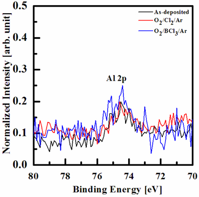
Figure 6 shows the Al 2p peaks of the XPS narrow scan spectra of the as-deposited and the etched HfAlO3 thin films in the O2/ Cl2/Ar and O2/BCl3/Ar plasmas. The Al 2p peaks were not deconvoluted, because their intensity was too low. The Al 2p peaks of binding energy were not shifted, but the intensity of increased peaks in O2/BCl3/Ar and in O2/Cl2/Ar plasma is higher, than in as-deposited film. This result means that the Al atoms of the HfAlO3 react with the Cl and O radicals. We supposed that the fluorine compounds, such as Al-Clx, remained on the surface of the HfAlO3 thin film.
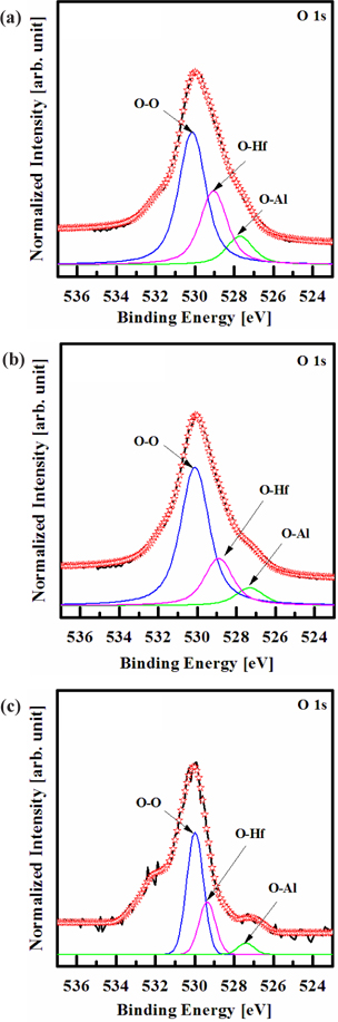
Figure 7 shows the deconvoluted peaks of the O 1s XPS narrow scan spectra for (a) the as-deposited films and the surface of the etched HfAlO3 thin films, in (b) the O2/Cl2/Ar, and (c) the O2/BCl3/Ar plasmas, respectively. For the O 1s peak, the peaks at 530.1, 529, and 527.7 eV correspond to those of O-O, O-Hf, and O-Al, which originate from the interface of HfAlO3 thin film. As shown in Figs. 7(b) and (c), the shoulder peaks of O-O, O-Hf, and O-Al decreased significantly in the O2/Cl2/Ar and the O2/BCl3/Ar plasmas, as a result of the preferential removal of Hf, Al, and O. However, when the HfAlO3 thin films were etched in the O2/Cl2/Ar and the O2/BCl3/Ar plasmas, the O 1s peak intensity at 530.1, 529, and 527.7 eV decreased, due to the formation of Cl-O bonds [20]. The intensity of the O 1s peak for the surface of the etched HfAlO3 thin film in O2/BCl3/Ar plasma was higher than that of the etched HfAlO3 thin film in the O2/Cl2/Ar plasma. This is due to the dramatic increase in the number of Cl-O bonds, resulting from the effective dissociation of the Hf- Al-O bonds by ion bombardment. Based on the XPS result, it was revealed that Hf, Al, and O were removed by the chemical reactions with the Cl radicals, and the physical bombardment of the Ar ions [20-22].
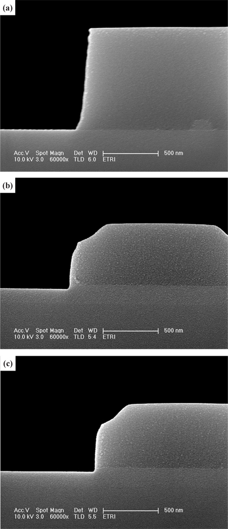
Figure 8 shows cross-sectional SEM images of the HfAlO3 thin film for (a) the as-deposited films and the surface of the etched HfAlO3 thin films, in (b) the O2/BCl3/Ar plasmas, at a process pressure of 1 Pa, RF power of 600 W, DC-bias voltage of - 150 V, and substrate temperature of 30℃. As shown in Figs. 8(b) and (c), a clean surface and side wall on the PR and HfAlO3 thin film were obtained with the PR mask erosion. It may be possible, in order to obtain a high etch rate and a vertical etching profile, to also change the etching conditions to be higher than the existing experimental. So, PR mask erosion was caused by the physical etch pathway. But, the experimental results showed that the vertical etching profile of the HfAlO3 thin film was obtained by the RIE using Cl radicals, due to the high etch rate of the HfAlO3 thin film.
The etching characteristics of the HfAlO3 thin film were investigated in the O2/Cl2/Ar and the O2/BCl3/Ar plasmas. The etch rate of the HfAlO3 thin film were 30.1 nm/min, 36 nm/min in the O2/Cl2/Ar(=3:4:16 sccm) and the O2/BCl3/Ar(=3:4:16) gas mixture. As the O2 fraction in the Cl2/Ar and BCl3/Ar plasmas was increased from 0 to 9 sccm, the etch rate of HfAlO3 thin film decreased. In order to the O2/BCl3/Ar(=3:4:16) gas mixture, the etch rate of the HfAlO3 thin film in the O2/BCl3/Ar plasma was higher, than in O2/Cl2/Ar plasma. Also, passivation layer formation occurred on sidewall, because of the small amount of O2. However, the etch rate of the HfAlO3 thin film increased, with the further addition of O2 gas. XPS was used to investigate the chemical states of the etched HfAlO3 thin films. The etching mechanism of the HfAlO3 thin film can be explained as follows: Ta interacted with the Cl radicals in the BCl3- and Cl2 - containing plasmas, but remained at the surface, due to the low volatility of Hf-Clx and Alx-Cly, which could be effectively removed with the help of ion bombardment.