Recently, resistive random access memory (ReRAM) devices on plastic have been intensively studied in the field of plastic based non-volatile memories, since they can easily be fabricated below the glass transition temperatures of plastic [1-4]. Compared to those on Si or glass, the performances of ReRAM devices on plastic have not been very satisfactory [5-8]. Hence, there have been many attempts to improve their performance [2,9,10]. More recently, the ternary compound, ZnOxS1-x, has emerged as one of the materials that could be used to improve the characteristics of plastic-based ReRAM devices [11,12]. Plastic-based ReRAM devices made of ZnOxS1-x exhibit retention properties comparable to those of ReRAM devices on Si or glass. On the other hand, doping in resistive switching materials and electrode materials are known to have significant effects on the memory characteristics of ReRAM devices [13-17]. The resistive characteristics of the materials are influenced by several factors, such as the combination of top/bottom electrode materials, and resistive material/ electrode materials. In addition, several factors affect the mode of resistive switching, which are classified into two types: unipolar or bipolar modes. In this study, therefore, we investigate the effects of doping and electrode materials on the performances of ReRAM devices made of ZnOxS1-x. Mn, as the dopant used in this study, is one of the most promising materials to facilitate the resistive switching of zinc manganese oxides [13,14,18].
Au and Cu bottom electrodes were deposited on a polyethersulfone (PES) plastic substrate by thermal evaporation, and the dc sputtering method, respectively. A resistive switching thin film with a thickness of 35 nm was then deposited on the electrode layers in an RF magnetron sputtering system with a watercooling unit. ZnOxS1-x and ZnOxS1-x : Mn as the resistive switching materials used in this study were sputtered from ZnOxS1-x and 1% Mn-doped ZnOxS1-x targets for 20 min, under a mixture of Ar and O2, at a pressure of 6.0 mTorr, with a sputtering power of 120 W, respectively. As the top electrodes, dot patterned Al electrodes with a diameter of 200 μm were deposited on the resistive switching thin film, by thermal evaporation. The electrical characteristics of the memory devices were examined with an HP4155C semiconductor parameter analyzer, at room temperature, in air.
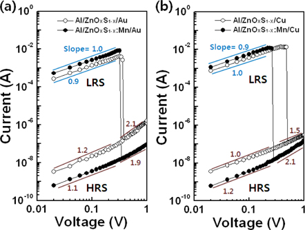
Figure 1 exhibits typical I-V curves of the Mn-doped and undoped Al/ZnOxS1-x/Au and Al/ZnOxS1-x/Cu devices in the positive voltage regions, with log scales, indicating unipolar resistive switching. Once a dc voltage is applied, tiny conducting filaments are formed, due to the alignment of the defects. In the low resistance state (LRS), the I-V relation exhibits Ohmic behavior, until these tiny filaments are ruptured by the Joule heating effect, which occurs in the high resistance state (HRS) [19-22]. The memory characteristics are achieved by switching between the LRS and HRS. Regardless of the Mn-doping, LRS of the ZnOxS1-x based ReRAM devices exhibits the Ohmic conduction behavior with a slope of ~1, which is concerned with the formation of conductive filaments in the devices, during the set process. The conduction mechanism in HRS is more complicated, which is in good agreement with a typical trap-controlled space charge limited conduction (SCLC), consisting of Ohmic regions (I∝V), the Child’s law region (I∝V2), and the trap-filled limit conduction region [2,19,20].
Compared with the undoped ZnOxS1-x based ReRAM devices, the magnitude of the current flowing in HRS of the Mn-doped devices gets lower; and consequently, the ratios of LRS/HRS become larger. Han et al. reported that Mn-doped samples become more resistive, because the doping of Mn ions depresses the concentration of intrinsic donors, such as interstitial zincs and oxygen vacancies in ZnO ceramics [23]. The Mn doping effect shown in this study is similar to the widening in the memory window of other metal doped-ReRAM devices, due to the increase in the resistivity of the HRS [13,17,18]. In this study, when the Mn ions are doped into the resistive switching material of ZnOxS1-x, the ratio increases from 2.2×10⁵ to 2.4×10⁶ for the Cu-bottom device, and from 5.9×10⁴ to 3.3×10⁵ for the Au-bottom devices.
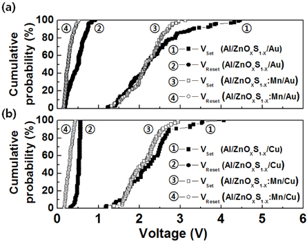
The distributions of the set and reset voltages reflect the effects of the Mn-doping and the electrode materials on the ReRAM characteristics, as shown in Fig. 2. In comparing the (a) Mn-doped and undoped Al/ZnOxS1-x/Au devices, and (b) Al/ZnOxS1-x/Cu devices, the Mn-doped devices exhibit narrower distributions of the set and reset voltages, than the undoped devices.
In the metal-doped resistive switching layer, the formation and rupture of the conducting filaments occur in a localized manner, due to the Mn ions around the conducting filaments; and consequently, the Mn-doped devices have relatively narrower distributions of the set and reset voltages [16,17]. Moreover, the Al/ZnOxS1-x/Cu devices show narrower distributions than the Al/ZnOxS1-x/Au ones. This is attributed to the higher affinity of copper to sulfur than that of gold, which forms more stable conducting filament paths near the electrodes of Cu [24].
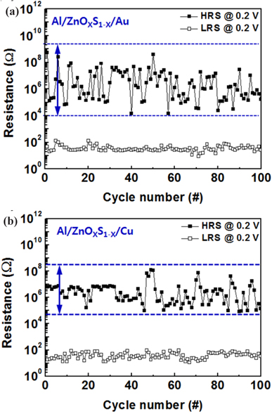
Because the distribution of the set/reset voltages is concerned with a rearrangement of filaments with a tree-like structure, stable conducting filament paths formed on the electrode are responsible for the narrower distribution of the set/reset voltages. Furthermore, careful comparison of the endurance characteristics of our undoped devices reveals that Cu is more appropriate as a bottom electrode material than Au for the ZnOxS1-x ReRAM devices, as shown in Fig. 3. The resistance of HRS in the Al/ ZnOxS1-x/Cu device fluctuates less significantly than in the Al/ZnOxS1-x/Au device, which is closely related to the narrower distribution of the set/reset voltages observed in the Al/ZnOxS1-x/Cu device.
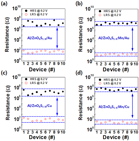
The resistance variations for each of the undoped [(a),(c)] and Mn-doped [(b),(d)] devices are represented in Fig. 4. The data points are the average values of the resistances (of ten devices with the same doping and electrode materials), obtained from measurements repeated 30 times. The dotted lines indicate the minimum and maximum values of the resistances, for each of the four different devices. For the Mn-doped devices, the ratios of the HRS to LRS are increased, but the variations in the resistances of the HRS and LRS are decreased (compared with the undoped devices), which are virtually the same as the results shown in Fig. 2. Consequently, the Mn-doping in the resistive materials causes an increase in the ratio of the HRS to LRS, and a decrease in the resistance fluctuations [13,17,25].
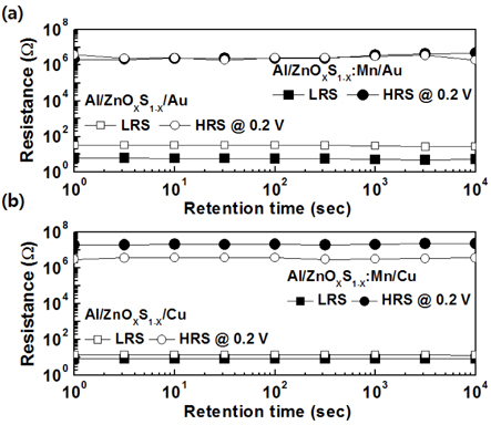
Figure 5 shows the retention properties of (a) the Mn-doped and undoped Al/ZnOxS1-x/Au devices, and (b) Al/ZnOxS1-x/Cu devices, measured at room temperature. Irrespective of the electrode materials, and with or without Mn-doping, the memory characteristics are maintained for 104 sec. The reliabilities of ZnOxS1-x based ReRAM devices are established at room temperature. Nevertheless, the temperature effect on the memory retention characteristics will need to be investigated, because the device temperature may increase during the operation. The effects of Mn-doping and the electrode materials on the ratio of the HRS to LRS are consistent with the results observed in Fig. 4. The Mn-doped ZnOxS1-x sputtered thin film turns out to be a suitable material for plastic-based high-performance ReRAM devices.
In this study, we investigate the effects of Mn-doping in the resistive switching material of ZnOxS1-x and electrode material on the memory characteristics of plastic-based ReRAM devices. The Mn-doping increases the ratio of the HRS to LRS, and narrows the distributions of the set and reset voltages, regardless of the electrode materials. For the ZnOxS1-x thin film, Cu is appropriate as an electrode material, due to the relatively higher affinity of copper to sulfur. The ratio of the HRS to LRS in the Al/ZnOxS1-x:Mn/Cu film is above 106. The metal-doping in the resistive materials, and the selection of appropriate electrode materials enable plastic-based ReRAM devices with higher performance to be achieved.