Recently, increases in world energy demand have focused research attention on renewable and clean energy sources, for which photovoltaic devices (PV) are promising examples. Organic materials are favorable candidates for photovoltaic technology because they offer the possibility of low cost production and flexible application opportunities [1-3].
Conventional silicon solar cells dominate the PV market, as they have demonstrated high power conversion efficiencies (PCE), up to 25% [4]. Organic hybrid solar cells based on semiconductor nanostructures (quantum dots) are among the most promising alternatives to traditional silicon solar cells. In a hybrid solar cell system, both semiconductor nanocrystals and polymers act as light absorbers and exciton generators [5].
One dimensional (1-D) nanostructures such as nanowires have been investigated in solar cell applications [6-9]. As the inorganic component of hybrid solar cells, wide band gap metal oxides, such as TiO2, ZnO, SnO2, and Nb2O5 have frequently been tested for photovoltaic properties [10-12]. Among all these materials, ZnO has attracted much attention in fabrication of solar cells due to its excellent properties such as low cost, direct band gap (3.37 eV), high exciton energy (60 m eV), high electron mobility (200 cm2 V−1 s−1), and non toxicity [13-15].
ZnO nanorod arrays can be easily grown on different substrates by different physical and chemical methods, such as metal-organic, chemical vapor deposition, magnetron sputtering, vapor liquid solid, chemical vapor deposition, and hydrothermal methods [16-21].
Among these techniques, hydrothermal is a facile method to grow nanorods normally to the substrate at low temperature (<100℃) [22]. It has been reported that ZnO nanorods (NRs) in solar cells improve light absorption and charge carrier collection [23-27].
The most successful organic solar cells consist of phenyl-C61-butyric acid methyl ester (PCBM), as an electron acceptor and a conducting polymer, poly (3-hexylthiophene) (P3HT), as an electron donor [28-35]. P3HT is an effective hole transport material and has high absorption coefficient in the visible region of the solar spectrum with high mobility of photo-generated holes (up to 0.1 cm2V−1s−1) [36, 37]. Several groups have shown that using 1-D ZnO nanostructures instead of ZnO film improves solar cell performance [38]. Y. Hames et al fabricated solar cells based on ZnO nanorods and investigated their photovoltaic properties [39]. They found that maximum power conversion efficiency for these devices is 2.44%.
To improve the cell efficiency, one can use light absorbers (or sensitizers). A successful way to do this is to use semiconductor nanoparticles (quantum dots) to sensitize the photo-electrodes. Since the optical properties of nano-particles depend on their sizes, they are good candidates for application in solar cells [40, 41].
Zinc sulfide (ZnS) is an important II-VI semiconductor inorganic compound which exists in two main crystalline forms (cubic and hexagonal). It has a direct band gap of 3.6 eV (bulk) at 300 K [42, 43]. This corresponds to ultraviolet (UV) radiation for optical inter-band transition, with a wavelength of 340 nm. ZnS is a promising material for optoelectronic device applications such as blue light emitting diodes, modulators, electroluminescent devices and photovoltaic cells. It has been extensively studied and most importantly, it is a nontoxic and more environmentally friendly material [44-46]. ZnS QDs can be fabricated by using various techniques such as spray pyrolysis, chemical bath deposition (CBD), successive ionic layer adsorption and reaction (SILAR) and so on. As a widely used, simple, low cost, versatile, large-scale production technique, the SILAR method has been used successfully to fabricate quantum dots.
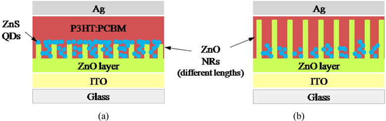
In this work we are going to further increase the cell performance by using ZnS QDs as light absorber material. In our device with structure of ITO/ZnO film/ZnO nanorods/ZnS QDs/P3HT/PCBM/Ag, both P3HT and ZnS QD cooperate in light absorbing.
2.1. Deposition of ZnO Seed Layer
Glass sheets (1.5×1.5 cm2) pre-coated with an indium tin oxide (ITO) layer were used as substrates. Prior to depositing the ZnO layer, these substrates were cleaned by using soap, de-ionized water, acetone, isopropyl alcohol and finally treated in UV ozone for 10 min, then dried with nitrogen. The zinc oxide layer used in this study was coated on substrates using a sol-gel spin-coating technique. The sol was prepared by dissolving zinc acetate [Zn (CH3 COO2) .2H2O] in ethanol (0.5 mol dm−3) and subsequently adding Diethanolamine (DEA) as a stabilizing agent into the solution. The molar ratio of DEA to zinc acetate was 6:5. Then, the resultant solution was stirred at 60℃ for 30 min to yield a clear and homogeneous solution, which served as the coating solution (sol) [47]. To deposit the ZnO layer, 50 μl of sol was dropped on the substrate and spin coated at 4500 rpm for 30 s and the film was dried at 150℃ for 2 min on a hot plate to evaporate the solvent and remove organic residuals. Finally the ZnO film was annealed at 450℃ for 2 h in a furnace. Since all steps of coating (adsorption, reaction, and rinsing) take place simultaneously during spin coating, this method does not require any rinsing step for elimination of residual organic materials [48]. The mean thickness of the ZnO film was about 70 nm.
To grow ZnO nanorods (ZnO NRs) on top of the ZnO layer, a hydrothermal growth process was carried out in a sealed kettle. ZnO seed layers were suspended in an aqueous solution of 0.001M Zn (NO3)2/0.1 M of NaOH upside down while the solution was stirred over a hot plate at 70℃. The pH of the growth solution kept at 11.33 [49]. In order to further investigate the dependence of the nanorod length on the growth period, the growth period was changed from 5 minutes to 1 hour. Finally, the samples were rinsed with de-ionized water to remove any residual organics and allowed to dry in air at room temperature. Hence we will label nanorods grown for 5, 10, 15, 20, 30 and 60 minutes by NR5, NR10, NR15, NR20, NR30 and NR60, respectively.
2.3. Synthesis of ZnS Quantum Dots
ZnS QDs were synthesized using the spin assisted successive ionic layer adsorption and reaction (SILAR) technique [50]. A 25 mM Zn (CH3COO)2 · 2H2O solution in ethanol was used as the source for the Zn2+ ions and a separate 25 mM Na2S.9H2O solution in DI water-methanol co-solvent (5:95 vol. ratio) was used as S2− source. To deposit the ZnS quantum dot layer on the ZnO film, at first, 50 μl of Zn2+ solution was dropped on the ZnO layer and spin coated at 4500 rpm for 30 s. Then 50 μl of S2− solution was dropped on the Zn-cation-adsorbed ZnO film substrate and spin coated at 4500 rpm for 30 s. The two-step procedure forms one SILAR cycle. Samples went through n SILAR cycles, herein referred to as ZnS (n). The ZnS film became darker as the number of SILAR cycles was increased. So all processes were repeated 4 times (n=4). The average thickness of ZnS QD film was about 24 nm. The spin assisted SILAR process eliminates the rinsing of excessive precursors and the additional drying process in conventional SILAR methods.
A polymer layer of Poly (3-hexylthiophene) (P3HT) and phenyl-C61-butyric acid methyl ester (PCBM) (1:1 wt/wt ratio) dissolved in1, 2-dichlorobenzene (ODCB) was coated on the ZnS QD layer by the spin-coating technique at 600 rpm for 50 s and subsequent thermal annealing was done at 150℃ for 30 min in a glove box under the nitrogen atmosphere. The thickness of this layer was 100 nm. Then a 100 nm thick silver front electrode was deposited on top of the film via vacuum evaporation in a high vacuum chamber (4×10⁻⁶ mb pressure). The active- area of the device with metal mask was 0.06 cm2. Figure 1 shows the schematic structure of fabricated photovoltaic devices containing ZnO NRs with different lengths.
2.5. Characterization Techniques
The structural characterization of ZnO NRs (grown for different periods) and QDs was measured by Philips (X’Pert Pro MPD) X-ray diffractometer with (40 kV and 40 mA) CuKα radiation (λ=1.5404 A°) in 2θ range from 30° to 70°. The surface morphological study of ZnO NRs with different growth periods and ZnS QD coated ZnO NRs was carried out using a Hitachi S-4160 FE-SEM. Optical absorptions were measured by using a Perkin Elmer UV-Vis spectrophotometer and current-voltage (J-V) characteristics of fabricated devices were measured at calibrated 1 sun illumination (AM 1.5, 100 mW/cm2) by using a solar simulator from Newport as light source with a Keithley voltage source.
3.1. Characterization of ZnO NRs and ZnS QDs
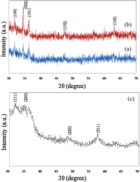
Figure 2 (a, b) shows XRD patterns of ZnO NRs with different growth periods (grown for 5 min and 1 h, respectively) but the same crystallinity. The crystalline nature of ZnO nanorods can be well indexed to known structures of hexagonal (wurtzite) ZnO, with lattice constants a=0.32498 nm, b=0.32498 nm and c=0.52066 nm [JCPS cardno.36-1451].
Five significant wurtzite ZnO diffraction peaks, (100), (002), (101), (102) and (103) appear at 2θ = 31.8°, 34.4°, 36.2°, 47.6° and 62.7° respectively. These results are in agreement with those of other authors [51-54].
It is evident that the (002) peak intensity of ZnO NRs grown for 5 min is lower than that of NRs grown for 1 h. This strongly enhanced (002) diffraction peak in Fig. 2(b) at about 34.4° indicates preferential growth of ZnO NRs along the c-axis. Moreover, the growth rate of ZnO along the c-axis is faster than those of other orientations because the basal plane (001) has the highest surface energy.
Diffraction patterns of ZnS QDs are shown in Fig 2(c). All the diffraction peaks from (111), (200), (220) and (311) respectively at 2θ= 28.9°, 33.5°, 48.1° and 57.1° are associated with reflections of the cubic zinc blende phase (sphalerite) of ZnS and are in agreement with other reports [55, 56]. These peaks were identified by using JCPDS (reference code: 01-080-0020) data for ZnS. The central broad hump is due to the amorphous glass substrate. The lattice parameters of the cubic structure are equal to a = b = c = 5.345 A°. The presence of broad peaks in XRD implies the presence of smaller particles [56].
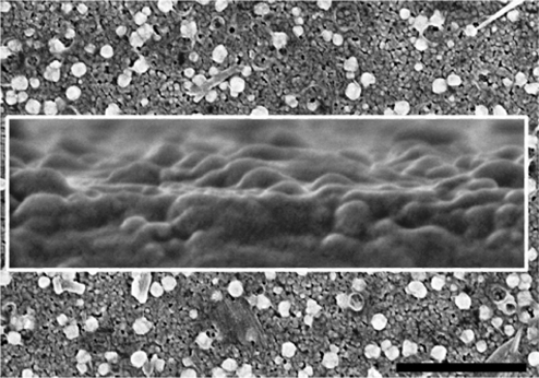
To investigate the effect of substrate on morphology of ZnS particles, first of all, these particles were synthesized on glass substrate. Figure 3 shows the SEM image of ZnS QDs grown on bare glass substrate.
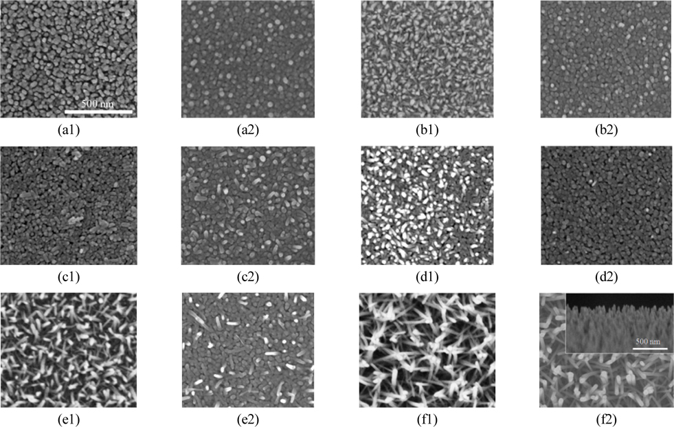
The surface morphology of ZnO NRs grown for different periods on the ZnO layer with (and without) ZnS QDs is shown in Fig. 4.
From Fig. 3 and 4, it can be seen that ZnO coated substrate has a significant effect on the morphology of ZnS QDs. In (a) and (b) samples (NR5, NR10) there are no void spaces between ZnO nanorods, because ZnO NRs are grown for short periods and there is still not a significant increase in their lengths. So, ZnS QDs cover the whole surface of samples during SILAR processes (a2 and b2). In contrast, in (e) and (f) samples as the growth period is long enough, the tip of nanorods are separated and ZnS QDs can penetrate in the space between NRs. Figure 4 indicates that after 15 min nanorods start to grow (Fig. 4(c1)), and uniform length distribution can be observed for nanorods grown for 20, 30 and 60 min (Fig. 4(d1), (e1) and (f1) respectively). The length of the nanorods grown for 20 min (Fig. 4(d1)) is 115 nm. When growth period of the nanorods increases to 30 min, the length of nanorods increases to 240 nm (Fig. 4(e1)), however, continuing to increase growth period of the nanorods up to 1 h, the length of nanorods increases to 350 nm (Fig. 4(f1)).
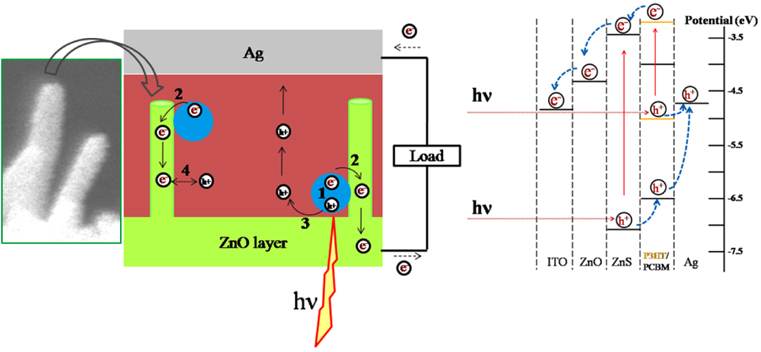
3.3. Working Principal and Recombination Pathways in System
The function of a quantum dot sensitized solar cell (QDSSC) is based on the formation of electron-hole pairs (exciton) in nanoparticle semiconductors by absorbing the incident light. Figure 5 shows the schematic diagram of exciton generation and charge transfers to different layers and corresponding energy level diagram for the device in our experiment. The situation of electronic energy levels is the most important factor governing efficient electron transfer between two semiconductors (and, consequently, photocurrent generation) [57]. As it can be seen from Fig. 5 (right), in our system the energy levels of components [39, 58 and 59] create a cascade structure between ITO/ZnO/ZnS/P3HT/PCBM which facilitates charge transfer from ZnS QDs to ITO contact.
The device is irradiated from the ITO side. P3HT and ZnS QDs absorb light and electron-hole pairs are generated over these layers (Fig. 5, path: 1). To extract the electrical energy, these excitons must be dissociated at interfaces and generated electrons have to be transferred to (ZnO layer) an electron conducting layer (Fig. 5, path: 2) in a proper way before they recombine with holes (Fig. 5, path: 4). The photo-generated holes must be extracted by (P3HT/PCBM) a hole conducting layer (5, path: 3) toward silver contact.
In such a structure, defects on the ZnO NR surface provide recombination sites (path 4) and decrease VOC in the QDSSC. The quantity of defects increases by increasing ZnO NR length through extending the growth period. Therefore, optimizing the growth period to obtain optimum nanorods strongly diminishes the recombination of injected electrons at ZnO/P3HT/PCBM interface. As a result, the suppression of the recombination of injected electrons and the facilitation of electron transfer due to the shortening of ZnO nanorods are the main factors leading to increases in VOC and efficiency in solar cells based on ZnO NRs.
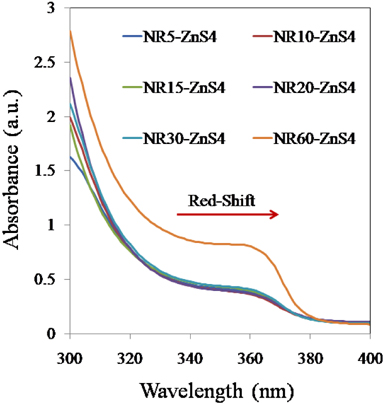
The UV-Vis absorption spectra of ZnO nanorods grown for different periods with ZnS QDs on them are shown in Fig. 6. This absorption spectrum indicates that long ZnO NRs (NR20, NR30 and NR60) have high UV absorbance properties at wavelengths below 320 nm compared to short ones (NR5, NR10 and NR15).
As shown in Fig. 6, there is a red-shift in the band-edge of ZnO NR60 in the UV-Vis spectroscopy compared with ZnO NR (5, 10, 15, 20 and 30). This red-shift indicates that increasing the growth period can influence the UV peak position of the ZnO NRs. On contrary, the difference in optical absorption between ZnO NR60 and other samples is possibly because of formation of more defects in nanorods during their fast growth [60, 61, and 49].
These defects can also be considered as suitable sites for sticking the ZnS QDs to ZnO NRs, resulting in an increase in generation of excitons.
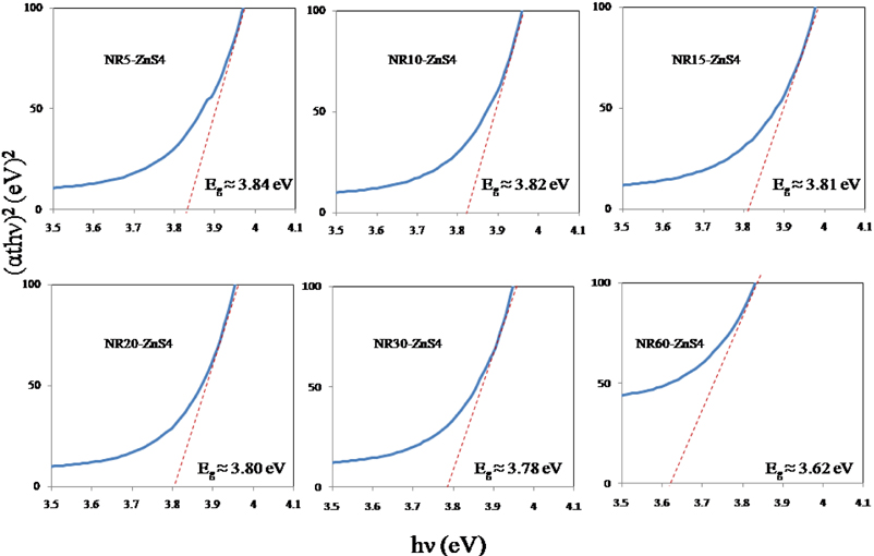
The red-shift of ZnO NR60 can be clearly observed in optical band gap estimation in Fig. 7. In order to determine the optical band gap energy (Eg), the standard relationship of

Finally, the band gap energy can be obtained by extrapolating the linear and sharply increasing portion of the curve and intercepting to the
As seen in Fig. 7, the band gap energy of the ZnO NRs slightly decreased by increasing the growth period. The significant decrease in the band gap energy of the ZnO NRs can be explained as follows. The longer growth periods can correspond to the formation of further defects in the nanorods. It has been reported that these defects in ZnO semiconductors can induce a defect level near the valence band [60].
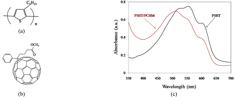
The optical characteristics of P3HT and the mixture of P3HT/PCBM (in a weight ratio of 1:1) layers were investigated by UV-Vis absorption spectroscopy. These materials with a concentration of 24 mg/ml dissolved in ODCB at 50℃ over night. Both P3HT and P3HT/PCBM layers were prepared on bare glass substrates by spin-coating technique at 600 rpm for 50 s and annealed 150℃ for 30 min. The thickness of these layers was 100 nm.
The chemical structures of P3HT and PCBM are presented in Fig. 8. Qualitatively, it was observed that the color of P3HT layer spin-coated in the absence of PCBM was purple and did not change during solvent vapor evaporation and annealing. In contrast, the color of P3HT/PCBM mixture was orange but became purple during solvent vapor evaporation for 50 s and annealing at 150℃. Figure 8(c) shows the UV-Vis absorption spectra of the P3HT and P3HT/PCBM layers.
It is obvious that P3HT exhibits the main absorption peak at 550 nm and two shoulder peaks at 520 nm and 600 nm. In contrast, the UV-Vis absorption spectrum of P3HT/PCBM shows the main absorption peak and one shoulder peak at 500 nm and 620 nm, respectively.
It is clear that the main peak in the mixture of P3HT/PCBM has a blue shift (because of solidification), and the shoulder due to vibronic transitions of P3HT/PCBM is decreased with respect to that of P3HT [38]. However, UV-Vis spectrum of the P3HT/PCBM presents lower absorption intensity than the absorption spectrum of P3HT.
The optical absorption spectra of P3HT/PCBM, which are blue-shifted during solidification (Fig. 8(c)), are strongly sensitive to solvent vapor evaporation and annealing processes.
Thus, the changes in the observed optical absorption edges, during solidification and solvent vapor annealing are mainly due to structural modifications in the P3HT/PCBM layer.
In addition, some studies mentioned that the absorption peak has red shift or blue shift when the inter-chain interaction between organic materials is changed [64]. One of the interesting features of organic polymer is that the band gap can easily be altered without changing its chemical components. It has been discovered that in several materials, the different arrangement in lateral chains can also result in different band gap structures. Moreover, changing the ratio of P3HT/ PCBM can change the gap as well [65]. Such a change, although prevented during the deposition of P3HT/PCBM films, is favored during solvent vapor annealing and provides beneficial effects on the photovoltaic device efficiencies.
3.5. Photovoltaic Properties of Samples
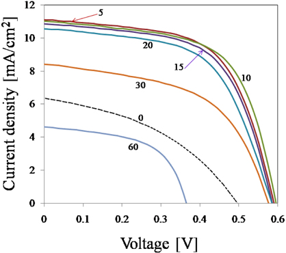
The photovoltaic (PV) properties of samples were investigated. In Fig. 9, the J-V characteristics of solar cells based on ZnO nanorods grown for various periods (with ZnS QDs on them) were compared. All devices were fabricated with the same active area of 6 mm2.
From the J-V characteristics, a clear performance enhancement was observed in the device based on ZnO NR10. For a growth period of 10 min, the short circuit current (Jsc), open circuit voltage (Voc), fill factor (FF) and efficiency were all improved. The detailed values of these parameters are given in Table 1.
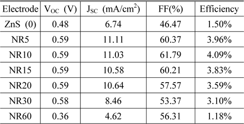
Photovoltaic performance of solar cells based on ZnO nanorods grown for different periods (covered with ZnS QDs) 100 mW/cm2 and (AM 1.5) simulated solar light
We analyzed solar cells performance based on ZnO nanorods grown for different periods (without ZnS QDs) and the maximum power conversion efficiency of those devices was obtained as 3.33%. Our experimental results show an apparent contribution of ZnS QDs and ZnO NRs to the cell performance. This contribution is found to be maximized when ZnO NRs grown for 10 min, indicating an optimum growth period for a device in our experiment condition is about 10 min.
It is clear that increasing the growth period from 5 to 10 min, leads to increase in fill factor and efficiency. The maximum power conversion efficiency (4.09%) was obtained for a device containing ZnO NR10. Further expanding the growth period, produces longer nanorods which promote light absorption, whereas this long pathway prepares more chance for electrons to recombine with holes. Therefore, in devices containing nanorods grown for more than 10 min, both efficiency and fill factor start to decrease. This indicates that nanorod arrays (NR10) serve as efficient transport pathways for electrons, and the parasitic losses in this device containing (NR10) are lower than other devices.
On the other hand, the high JSC, FF and ultimately higher efficiency of the device with ZnO NR10 can be attributed to the strong absorption of light and efficient charge transport through a facile one-dimension pathway after successful exciton dissociation [66].
The decrease in VOC from 0.59 V to 0.36 V for NR60 is attributed to creation of longer electron pathway. It can be concluded that increasing the length of nanorods (NR60) has 2 opposite effects on the cell performance: (1) light absorption is increased; meanwhile (2) photo-generated electrons find more chance to recombine with holes, which leads to decrease in VOC.
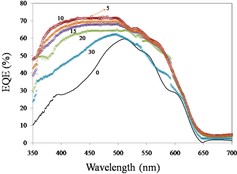
External quantum efficiency (
It is clearly observed that the EQE value of hybrid solar cells (containing ZnO nanorods and ZnS QDs) in the range of 400-500 nm (corresponding to 2.47-3.1 eV) is almost constant (70%). Photons at these wavelengths are converted and extracted more efficiently as light is absorbed closer in active layers. At short wavelength region (<400 nm), the EQE varies slightly in accordance with the spectral dependence of reflectance from ZnO nanorods. For hybrid device containing (ZnO NR10)), EQE is higher, establishing charge carrier generation in active layers (ZnS QD layer on ZnO nanorod and P3HT).
The increase in EQE for hybrid devices can simply be attributed to an increase in light absorption because there are 2 active layers in hybrid cells and only one active layer in the device without ZnS (with ITO/ZnO/P3HT/PCBM/Ag structure).
In summary, ZnO nanorods (NRs) grown for various periods on the ZnO seeds/ITO substrates were fabricated. In the fabricated hybrid solar cell, P3HT and ZnS QDs cooperate in light absorption. The performance of our hybrid solar cell with the configuration of ITO/ZnO film/ZnO NRs/ZnS QDs/P3HT/PCBM/Ag achieving 4.09% has been demonstrated using ZnS QDs. Without the use of ZnS QDs as light absorber layer, the maximum power conversion efficiency of 3.33% was achieved.