Regardless of the advantages of light-emitting diodes (LEDs), including high energy efficiency, long lifetime, vivid colors, high reliability, environmental protection, and safety, the external quantum efficiency (EQE, ηext) is still an important issue that must be addressed to meet practical needs [1, 2]. The EQE of an LED can be expressed as the product of the current injection efficiency (CIE, ηinj), internal quantum efficiency (IQE, ηint), and light extraction efficiency (LEE, ηextr) [3, 4]. The LEE of an LED depends strongly on the critical angle θc for total internal reflection at the interface between the two media, which is determined by Eq. (1) as follows:
where n1 and n2 are the refractive indices of the media on the incident and transmitted sides respectively.
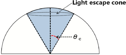
The LEE is defined as the fraction of photons generated in the active region of the semiconductor that escape into free space. As shown in Fig. 1, the LEE based on the light-escape cone from the LED chip can be determined with Eq. (2) using θc:
Gallium nitride (GaN) is most commonly used for LED chips, and emits blue light. In the case of the GaN/air interface, unfortunately, the refractive index of GaN is relatively large (n = 2.54) compared to that of air (n = 1). This large refractive index mismatch results in a narrow light-escape cone with θc of 23.18°, as calculated with Eq. (1). Light impinging on the interface outside the extraction cone is subject to total internal reflection and eventually reabsorbed in the semiconductor or its metallic contacts [5, 6]. A great amount of the light emission from quantum wells is lost within the GaN layer due to light confinement and subsequent reabsorption, which results in a temperature increase in the
Index matching via an intermediate layer between the LED chip and the air has been used to increase the LEE [13]. An encapsulant is a type of intermediate layer for index matching consisting of a phosphor and an epoxy to fix the phosphor. For encapsulants with intermediate refractive indices, θc increases and ultimately LEE increases. There have been many studies of encapsulants addressing modification of the shape of the encapsulation [14], addition of particles into the encapsulant [15], the effects of the hardening characteristics of the encapsulant [16], the development of encapsulants with high refractive indices [17, 18], and multilayered encapsulation [19]. Most of these studies have focused on spherical encapsulants, but because of the current trend of using high-power, multichip LED packages, the need to study flat encapsulants has arisen.
For this reason, this study is focused on how to increase the LEE of LED packages in which the top surface of the encapsulant is flat. In this study, the refractive index of the encapsulant was varied (1.41 and 1.53) and also doublelayer structures featuring the two indices (1.41/1.53) were investigated by varying the shape of the interface between the two among flat, concave, and convex. We investigated the change in the light output according to the experimental conditions, from the viewpoint of the critical angle and Fresnel reflection. The optical properties of the LED package were measured using an integrating sphere to investigate the change in light output. The measured light output was compared to results simulated using three-dimensional (3-D) ray-tracing to ensure the validity of the new encapsulant design.
2.1. Constructing the LED Packages
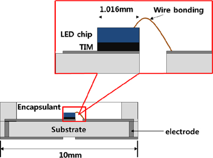
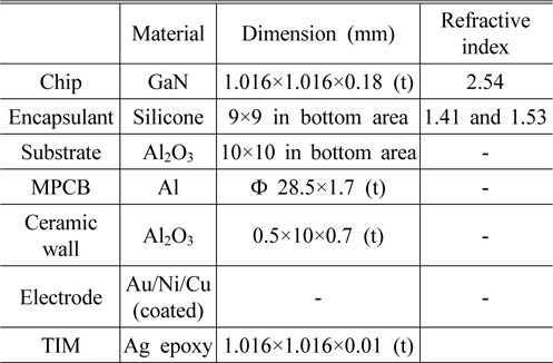
Table 1 shows the general specifications for each component of the single-chip LED package that was used in this study. A vertical GaN chip was used to obtain blue emission light, and was covered with a flat encapsulant as shown in Fig. 2.
[TABLE 1.] General specifications for each component of the LED package
General specifications for each component of the LED package
Each LED chip was bonded to an Al2O3 submount (ceramic substrate) using Ag epoxy as a thermal interface material (TIM). The submount was made of low-temperature cofired ceramics (LTCCs) consisting mainly of alumina. Negative electrodes were located a top the LED chips and were electrically connected to the circuit lines using Au wire bonding. Positive electrodes (Au/Ni/Cu coated) were located on the bottoms of the LED chips and were electrically connected to the circuit pads on the upper surface of the submount using a TIM. 1.4-mm-thick ceramic ribs to protect the chip were attached to the substrate using ceramic paste. The encapsulant was dispensed to fill inside the ceramic package and form a flat top surface, and was hardened using a two-step heat treatment (150℃ for 3 hours, followed by 200℃ for 2 hours). In the case of the double-layer structure with two different encapsulant materials, the upper layer was dispensed after the lower layer had hardened. The refractive index of the LED chip was 2.54, while the refractive index of the encapsulant was varied using values of 1.41 and 1.53.
2.2. Measurement of LOP of the LED Package
We put the LED package into an integrating sphere 1 m in diameter to measure the LOP of the package. The light flux emitted from the package was scattered onto the inner surface of the integrating sphere and measured by the detector. The measurement was conducted under operating conditions of 350 mA and 3.2 V.
2.3. 3-D Ray-tracing Simulations
We used 3-D ray-tracing simulation software in which the light distribution and output were measured by detecting the number of the rays captured at the receiver. The light distribution was analyzed using ray-tracing simulation based on the Monte Carlo method and Snell’s law.
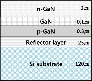
Figure 3 is a schematic drawing of the LED chip, which consists of Si substrate, reflector layer,
The electrodes on top of the LED chip were not considered, for the simplicity of the calculation. The emission spectrum of the LED chip had a peak at 460 nm and followed a Gaussian distribution between 360 nm and 560 nm with a FWHM(full width at half maximum) of 50 nm. Alumina, the material used for the substrate and ribs, has a reflectance of 80%. The thickness of the encapsulant, which had a transmittance of 97%, was 1.4 mm. Fresnel reflection was assumed to occur at material interfaces with different refractive indices such as chip/air, chip/encapsulant, and encapsulant/air. For the ray-tracing simulation, 4 million light rays were generated at the bottom of the LED chip and their optical paths traced using the simulator, which were measured by a detector which was distributed on the inside of the integrating sphere (diameter 1 m).
3.1. LOP according to the Encapsulant Design (Measured and Simulated)
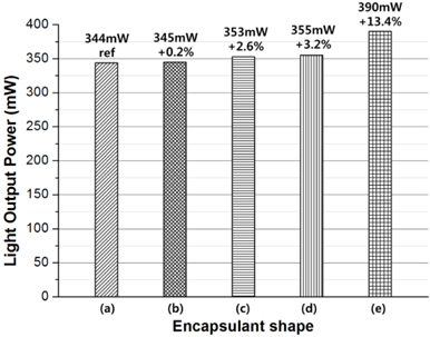
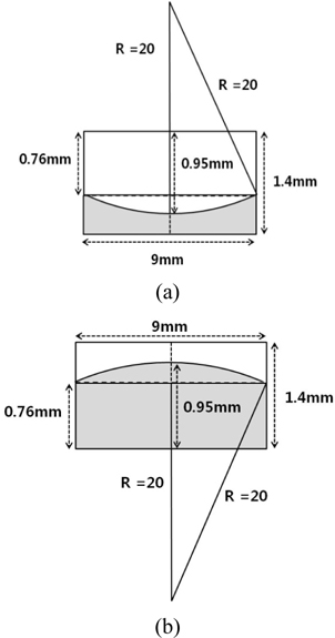
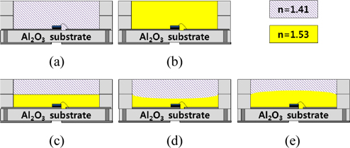
Figure 4 shows schematic drawings of five different designs for the encapsulant. In cases (a) and (b), the package was filled with an encapsulant with a refractive index of 1.41 and 1.53 respectively. The thickness of the encapsulant was 1.4 mm. In cases (c), (d), and (e), two different encapsulant materials with refractive indices of 1.41 and 1.53 were stacked in the form of a double layer. The total thickness was 1.4 mm, but the shape of the interface between the stacked layers was different in each case: (c) was flat, (d) was concave, and (e) was convex.
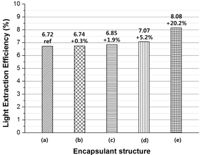
Figure 5 shows the results of the measured LOP using an integrating sphere. The case of the double-layer encapsulant with a convex interface, (e), showed the highest value of 390 mW, which is 13% higher than the 344 mW of case (a). To investigate and analyze the change of the LOP according to the design of the encapsulant, a 3-D ray-tracing simulation was conducted.
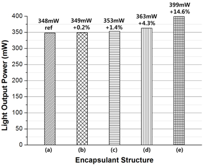
Figure 6 shows the simulation data of the LOP of the LED package according to the encapsulant design. Figure 7 is a schematic drawing of the curved interface, in which the radius of curvature
To understand the effect of the curved interface of the double-layer encapsulant on the LOP of the LED package, we investigated related factors such as the LEE, the lightescape cone for θc, and the Fresnel reflection loss based on the ray-tracing simulation.
3.2. Increase of the Critical Angle θc at the Curved Interface
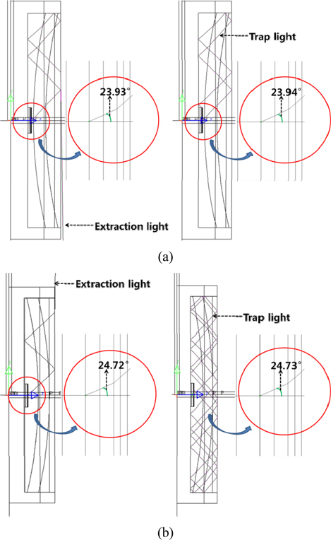
Figure 8 shows the optical paths of some reflected rays with incident angles beyond the original critical angle (23.18°) at the curved interface, which was investigated using 3-D ray-tracing simulation. In the cases of concave (a) and convex (b) interfaces, critical angle θc was seen increase to 23.93° and 24.72° respectively. Figure 8 shows that some light rays which were reflected at the curved interface can escape the chip, even though their original incident angle was greater than 23.18°. Since this increase in θc is due to the characteristic of the curved interfaces, we define the increased θc at the curved interfaces as the ‘effective critical angle’. The basic cause of the effective critical angle can be explained in two ways. First, owing to the curved interface, a normal line at its point of tangency tilts a little, which changes the incident angle and increases θc at the curved interface. Secondly, rays reflected at a free surface have a decreased incident angle at the curved interface, which enables some of the reflected rays to escape the chip.
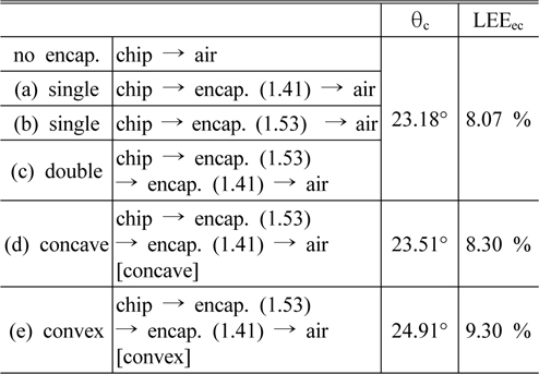
To consider the geometrical factors, we have obtained the effective critical angle θc at 9 different positions at the interface and averaged them, to obtain 23.51°and 24.91° respectively. We have used these average values of the effective critical angle for Table 2.
[TABLE 2.] Calculation of LEEec using the effective critical angle θc obtained in Fig. 8

Calculation of LEEec using the effective critical angle θc obtained in Fig. 8
Table 2 shows that the LEEec values of (a), (b), and (c) are same as in the case of no encapsulation, because the same θc applies. It should be noted that θc mentioned in Table 2 is the critical angle at the free surface, which depends on the refractive indices of the chip and air only. In other words, the intermediate media between the LED chip and the air do not affect the critical angle at the free surface, which is an optical characteristic for a multilayered structure with flat interfaces.
The effective critical angles increased to 23.51° and 24.91°, respectively for (d) and (e), which resulted in LEEec values of 8.3% and 9.3% respectively, which were higher than in other cases (8.07%).
3.3. Fresnel Reflection Loss at the Curved Interface
In general, when a wave reaches the boundary between two media with different refractive indices, one part of the wave is reflected and the other is transmitted, with the sum of the energies of these two waves equal to that of the original wave. It is well known that the light is split into
where
On the other hand, when multiple interfaces are involved the reflectances for
where
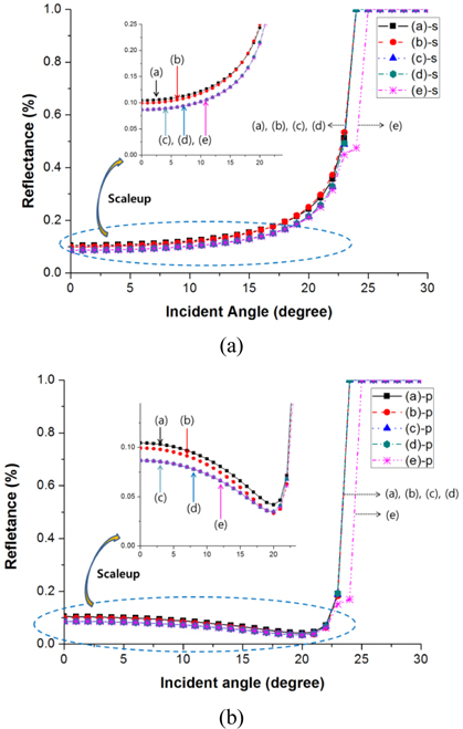
Figure 9 shows the Fresnel reflectance according to the incident angle. We input the incident angle into Eqs. (3) and (4) with an increment of 1° in the range from 0° to θc, which was converted to reflectance using Eqs. (5) and (6). The Fresnel reflection loss was determined using Eqs. (7) and (8) with the reflectance values at every interface. In the cases of the curved interfaces, (d) and (e), the effective θc was obtained using a 3-D ray-tracing simulation, as mentioned above.
Two different features were found in Fig. 9, according to the range of the incident angle. For the range between 0° and 30°, both
[TABLE 3.] Determination of the total LEE by multiplying the transmittance and the LEEec

Determination of the total LEE by multiplying the transmittance and the LEEec
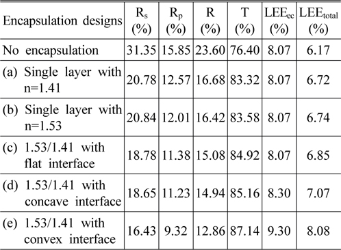
In Table 3 we determined the total LEE by multiplying the transmittance and the LEEec. In Table 3 the total reflectance of the rays passing through the encapsulant was defined as
Therefore, the total transmittance of the rays passing through the encapsulant was defined as
It can be seen in Table 3 that
In Table 3 we define the total light extraction efficiency LEEtot as follows:
where LEEec is the light extraction efficiency determined by the light-escape cone using Eq. (2), and
By experiment and 3-D ray-tracing simulation, we have shown that the LOP of an LED package was most effectively enhanced by structure (e) using a double-layered convex-interface encapsulant, resulting in a 13.4% increase compared to a single-layer encapsulant structure (a). The enhancement mechanism was explained in two ways.
First, from the simulation it could be seen that the critical angle was the highest at 24.91° for (e), compared to 23.18° for (a), which was explained by the concept of the effective critical angle at a curved surface. Second, total transmittance