Three-dimensional heterogeneous integration based on through-silicon-via (TSV) has emerged as a key approach to continue power and performance scaling of next generation systems. Three-dimensional integrated circuit (3D IC) floorplanning is an effective means to explore architectural design space of 3D ICs during an early stage of design. Based on a limited amount of information available in the given architectural design, the goal is to quickly build a block-level 3D layout of the architectural modules while optimizing the metrics of concern and generate feedback on its quality. This feedback is then used by architects to help improve the architectural design in an iterative fashion. A key aspect of 3D IC floorplanning in this scenario is to provide as much accurate and practical information of the final 3D design as possible within the shortest amount of time.
3D IC floorplanning poses several new challenges. First, there is a crucial need to consider the impact of TSVs in the floorplanning solutions. TSVs are not only the I/O and power/ground (P/G) ports of the blocks, but they also introduce many unknowns in power, performance, reliability, and yield of 3D ICs. For example, TSVs can modulate the power supply noise and thermal profile of a 3D stack. Hence, TSV-aware and TSV-unaware 3D floorplanning may lead to very different thermal/noise profile for the entire 3D stack.
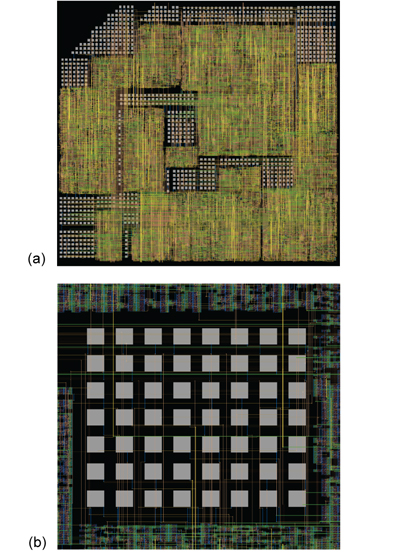
Second, designers can consider the TSV usage and their placement in between the blocks more accurately when the detailed layouts of individual blocks are available (=hard IPs). However, the problem is more challenging at the early stages of floorplanning when detailed layouts, and hence the TSV profile of individual blocks, are not available (=soft IPs). This unknown may pose a significant challenge in the early stage TSV-aware floorplanning in terms of the accuracy in system metrics.
Third, integrating the same set of blocks in 2D vs. 3D can lead to different floorplanning solutions as the 2D vs. 3D designs have very different thermal and power delivery network properties. The die-to-die coupling in effects, such as thermal and voltage drop (IR noise), can change the physical interaction between blocks when they are integrated in 2D vs. 3D.
We thus identify the following requirements in modern 3D IC floorplanner: 1) TSV planning must be an integral part of 3D floorplanning. TSV-aware floorplanning helps designers make more informed decision based on more accurate prediction of the final 3D IC design, 2) 3D IC floorplanning evaluation methodology must cover a wide range of important metrics including both the conventional metrics, such as power, performance, and thermal, but also the newly emerging concerns, such as TSV stress, coupling, EM, etc. 3) 3D IC floorplanner must handle a wide range of heterogeneous blocks including soft and hard IPs.
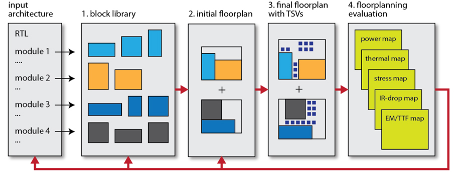
Fig. 1 shows a typical flow for 3D IC architectural floorplanning. Given an initial register-transfer level (RTL) description of the input architectural design, we perform the following steps.
Step 1: Block characterization and library management.
For each functional module (=soft IP) in the RTL, we build a set of physical implementation options that vary in terms of area, performance, power, and TSV usage. In case of TSV usage, we characterize the effects of 1) connecting a variable number of I/O ports to other modules in different tiers, and 2) using a variable number of power/ground TSVs in the block. We also provide sensitivity analysis of each module under the noise, thermal, and process variation consideration. This step can be performed by the system designer (for soft-IPs) or by the vendors (for both soft/hard IPs) and results can be provided in terms of numerical tables (for detail floorplanning) or relative values (for quick evaluation).
Step 2: Block selection and initial 3D floorplanning.
The next step is to select a block from the library for each module in the RTL based on the area, performance, power, and reliability constraints. Once the block selection is completed and their connections are identified, we build an initial 3D floorplanning, where we pack the blocks to minimize the overall area, wirelength, and/or other primary objectives. For this step, we can either rely on floorplanning experts (=manual floorplanning), or utilize an automatic 3D floorplanner, such as sequence pair plus simulated annealing approach
Step 3: TSV insertion and final floorplanning.
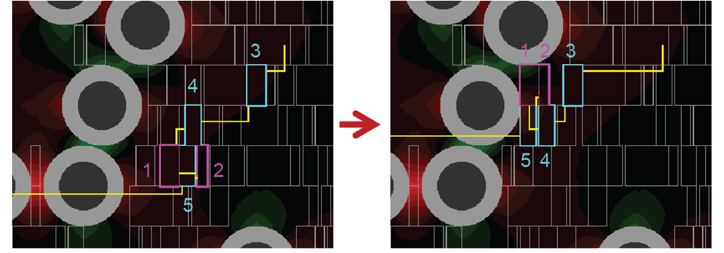
For each 3D net, we add one or more TSVs based on a Steiner tree that connects the blocks in the net. TSVs are then inserted into the nearest available whitespace while forming either 1D or 2D arrays as shown in Fig. 2. We impose an upper limit on the size of these TSV arrays based on TSV coupling [1] and mechanical stress [2] consideration. In case there is no available TSV array nearby, we expand the floorplan to add more whitespace.
Step 4: 3D floorplan evaluation.
Once the final 3D floorplan is obtained with all TSVs inserted, we add on/off-chip power delivery network (PDN). We first build a 3D mesh with on-chip power and ground lines and TSVs based on the current demand of the blocks. We also insert P/G C4 bumps and redistribution routing layer (RDL). The goal is to quickly extract its 3D resistive network and calculate IR-drop and EM failure [3] in the PDN at floorplanning-level. Next, we evaluate the final 3D floorplan in terms of performance, power, and electrothermo- mechanical reliability. Static timing analysis is done based on the pin-to-pin delay values available from the library. We also perform power analysis based on statistical simulation of the blocks and build a power map. This map is then used to obtain thermal profile of the 3D floorplan, which considers the TSVs in the arrays as heat conducting paths to the heat sink. We also perform TSV stress-induced mechanical reliability analysis of the substrate and EM analysis for our PDN.
Based on the feedback from 3D floorplanning, architects may either re-floorplan, replace blocks, or re-optimize the overall architecture. The iterative process is repeated until a desired architecture is obtained.
In order to accomplish our goals in 3D IC architectural floorplanning, we identify the following specific needs.
Need 1: Block-level modeling.
The goal is to characterize the power, performance, and reliability factors of an architectural block, considering the effects of different placement options and TSV (signal and P/G TSVs) usage. The characterization needs to focus on 1) usage of TSVs in I/O ports, 2) IR drop, 3) thermal behavior, and 4) sensitivities of power, performance, noise margin of the block to temperature and voltage variations.
Need 2: TSV insertion and management.
The goal is to add signal and P/G TSVs either in between the hard IP blocks or inside soft IP blocks so that the given constraints on coupling noise, thermal, clock skew, mechanical reliability, power supply noise, yield, etc., are satisfied.
Need 3: Chip/package co-evaluation.
The goal is to be able to integrate the block-level properties to create chip-level properties and evaluate the final 3D floorplan. We aim to improve the accuracy and speed to allow fast evaluation of many floorplan solutions. In addition, the following supporting structures must be added to the floorplan solutions to evaluate the quality more accurately: 1) TSVs inserted in an array or block styles for both soft and hard IPs, 2) block-level on-chip power distribution network, and 3) off-chip power delivery planning (C4 bump placement and routing). The tool then must compute the maximum frequency and overall power consumption. Moreover, die-by-die maps for various reliability metrics including temperature, IR-drop, mechanical stress, and EM must be generated. The runtime of floorplan evaluator will need to be kept low to allow evaluation of many floorplans (=from many architectural designs) within reasonable amount of time. In addition, the accuracy of metrics measured from the given floorplans must be sufficiently accurate and realistic to allow better judgment during 3D architectural solution space exploration. The following sections provide details on these research needs.
>
B. Need 1: Block-Level Modeling
As we are interested in block-level 3D ICs, the signal TSVs corresponds to I/O ports. The static timing/power analysis helps estimate power and performance of a block. However, there exist different unknown factors as the final placement of the block in the 3D floorplan is not available during this characterization step. Therefore, we need to predict the different possible conditions and generate a range of power/performance for the blocks (instead of one). For each of these conditions, statistical analysis can be further used to account for the effect of process variations in devices, wires, and TSVs. The goal is to identify the key sources of unknowns and characterize their effects. This research needs solutions for the following issues:
A different 3D floorplan leads to a different number and choice of 3D I/Os for a particular block. The performance factors of a port depend on whether it uses TSV or not. Moreover, depending on the logical structure of the block, different ports have different timing/power criticality. Hence, we need to compute the power/performance of a block as a function of the number of 3D I/O ports. We can use stochastic 3D wire-length model considering stochastic placements of the TSVs to account for the non-determinism in the impact of interconnect (2D and 3D) parasitic as the detailed internal layout of the block and inter-block TSV placements are not available at this stage.
The IR drop within a block depends on the current drawn and effective resistance of the power-ground network. We can estimate effective average current using power analysis, which depends on the logic and design of the block. Moreover, depending on the P/G TSV usage of a block and its final placement in the 3D stack, the IR drop can vary significantly for the same power drawn. Hence, we need to characterize the sensitivity of IR drop of individual blocks to the number and usage of TSVs. The goal is to consider a regular or irregular (stochastic) placement of the P/G TSVs and use that to generate a statistical estimate of IR drop (a range of IR drop map and a peak IR drop metric) as a function of the number of P/G TSVs.
The steady-state temperature of a block depends on its logic (power) and placement in the 3D floorplan which defines the thermal resistance (e.g., distance from the heat sink, chip edge, etc.). The effective thermal resistance of a block also depends on TSVs usage (P/G and signal) as they act as good conductor of heat. We must perform a blocklevel thermal analysis to estimate a range of peak temperature of a block based on different placement in the 3D stack.
4) Estimation of Power/Performance Sensitivity
The IR drop and temperature significantly affect the performance and power of a block. However, depending on the logic/circuit design, the block temperature and voltage noise may have very different impact on the overall performance. Therefore, it is critical to obtain a metric for individual block that provides sensitivity to voltage and temperature noise. This voltage and temperature sensitivity metric can also be provided in the form of a 2D map to reflect the sensitivity of different spatial locations within the block. The sensitivity map can be generated during the power, performance, and reliability characterization of the individual blocks.
>
C. Need 2: TSV Insertion and Management
The main focus is to study optimal location of TSVs in the given floorplan so that the design quality improves while the associated reliability issues are considered. In most cases TSVs form arrays instead of being isolated individually. Thus, our goal is to compute the proper number of TSVs in each array. Since TSVs are added onto the whitespace in between blocks in floorplan, our next goal is to manage whitespace so that we can place TSVs at desired locations as much as possible.
1) TSV Array Sizing under Reliability
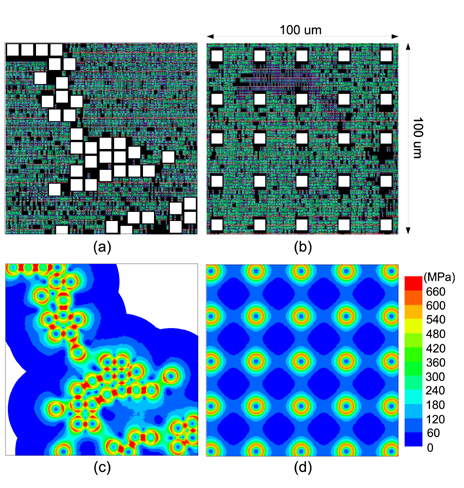
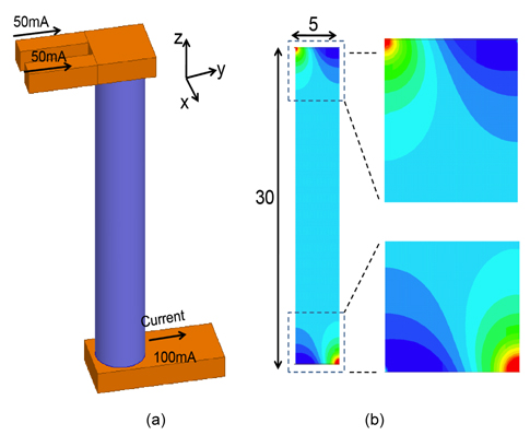
The TSVs in the arrays electrically couple with each other, causing performance loss and potential logic failure [1]. In addition, if TSVs are gathered in a confined space, the TSVinduced stress caused by copper-silicon coefficient of thermal expansion (CTE) mismatch causes performance and power variations to devices nearby [4] (see Fig. 3) and impose structural reliability concerns to the substrate [2] and TSVs themselves [3] (see Fig. 4). Keep-out-zone can alleviate these issues [5] but comes with a significant area overhead. The goal in this research is to consider all these factors and determine the proper size of the TSV arrays so that they do not cause area and reliability problems when created in 3D floorplan. Basic finite element analysis (FEA) simulations and linear superposition principle method will be used to analyze the reliability issues for various candidate dimensions.
2) TSV-Aware Whitespace Management
Given a 3D floorplan with functional blocks packed into multiple planes, the whitespace in between the blocks is the prime target for TSV insertion. The ideal location of TSVs used in a given net can be determined by constructing a 3D Steiner tree under certain objectives, such as wirelength, performance, etc. However, the ideal location of TSVs in the tree may not always coincide with whitespace location. In this case, we need to assign the TSVs to nearby whitespace (or even add new whitespace if no space is available). We must solve this TSV-to-whitespace assignment problem so that all TSVs from all nets are assigned to all whitespace simultaneously, instead of handling one net at a time.
This kind of concurrent approach usually requires prohibitive runtime, and one can adopt approximation algorithm to handle the complexity and provide fast turnaround time during architectural design space exploration. We can perform whitespace pre-adjustment, where the whitespace in the initial 3D floorplan are shifted aroundwhile maintaining the overall footprintto make more room for more popular spots in the floorplan before starting TSV assignment. We can use the shapes and upper bounds obtained from the block-level modeling research while populating whitespace. In addition, we can consider “passthrough TSVs” to be inserted into soft IPs so that these TSVs are added simply to allow connections between other blocks in the floorplan. Due to the area overhead involved, this will be done only when there is clear benefit in terms of area and wirelength.
>
D. Need 3: Chip/Package Co-evaluation
Once a full-chip 3D floorplan is built with TSVs inserted at proper location and its connection to the underlying package structure defined, our next goal is to evaluate the entire chip/package design in terms of power, performance, and electro-thermo-mechanical reliability. The research on this topic must target multi-physics reliability issues in 3D including mechanical stress, IR-drop, and EM issues.
1) Full-Chip/Package Stress Co-analysis
Given a 3D flooplan with all functional and TSVs blocks added and C4 bumps, underfill, and package substrate also added, our objective is to obtain the mechanical reliability report of the entire chip/package structure. This report consists of full-die reliability map for each die in the 3D IC and full-scale reliability map for the chip/package interface. Our recent works allow us to obtain full-die substrate reliability [2] and TSV interfacial crack growth [3] maps for a given die in a 3D IC in isolation, i.e., the contributions from other neighboring dies or the package are ignored. We can extend this work to consider the stress from package caused by CTE mismatch between the materials used at the chip/package interface and warpage. Linear superposition will need to be validated for the basic structure that contains multiple TSVs, micro-bumps, C4 bumps, and underfill. Full-chip/package scale reliability map using von Mises stress metric will need to be built based on the parametric library we build using FEA simulations. The goal here again is to quickly generate reliability maps for the given 3D floorplan at block-level to allow efficient architectural design space exploration.
2) Full-Chip/Package IR-drop Co-analysis
Given a 3D flooplan with all functional and TSVs blocks placed and the on-chip 3D PDN, P/G C4 bumps, and package-level PDN inserted, the goal of this research is to perform IR-drop analysis for the entire chip/package PDN and identify power delivery hotspots in the floorplan. Instead of performing detailed optimization on our on/offchip PDN, we must build a few candidate options with varying on-chip P/G mesh density, P/G TSV usage, and P/G C4 bump usage. Given a 3D floorplan, we add current sources to our PDN and perform IR-drop in the resistive network. Our recent work [6] allows us to use Synopsys PrimeRail to extract and stitch resistive networks from the individual dies in the 3D IC and from the package. We can adopt this tool and further refine it to perform floorplanlevel chip/package 3D IR-drop analysis.
3) Full-Chip/Package EM Co-analysis
In 3D ICs, the mechanical stress caused by the CTE mismatch between TSV and chip silicon substrate poses additional concern to the EM issue in the nearby BEOL wires. In addition, the CTE mismatch between chip substrate, packaging substrate, C4 bumps, and under-fill further exacerbates the stress problem and thus the EM issue. Moreover, the signal paths arriving at the C4 bumps through their package pads are rerouted in the RDL layer and connected to the local metal layers and vias. The significant size mismatch between these routing resources further aggravates the electomigration problem at the smaller scale interconnects due to the steep current density gradient and serious current crowding.
The smaller footprint and higher device density of 3D ICs put higher current demand on each power/ground (P/G) C4 bumps and P/G TSVs that are connected to them. Our recent work [7] presented a study of current crowing in P/G TSVs and its long-term impact on IR-drop and aging (see Fig. 5). This study can be extended to study the impact of floorplanning, which is important because floorplanning update leads to the changes in the current consumption pattern among the blocks.
Architectural floorplanning is a useful method to evaluate the quality of 3D IC designs at a very early stage of design process. This article presents several key research needs in 3D IC floorplanning including block-level modeling, TSV insertion and management, and chip/package co-evaluation. The physical and geometric information available through floorplanning solutions allow the evaluation of several important metrics including power, performance, and electro-thermo-mechanical reliability. A key aspect of 3D IC floorplanning is to provide as much accurate and practical information of the final 3D design as possible within the shortest amount of time.