Currently, smartphone use continues to increase and is now an essential part of people’s daily lives. Mobile applications that utilize long-term evolution (LTE) of 3rd generation partnership project (3GPP) are now popular because of highly responsive mobile voice and data services. However, the development of new mobile communication systems such as LTE-Advanced is required to satisfy demands for high-speed multimedia data communications such as real-time video streaming. The LTE-Advanced system offers a peak data-rate of 1 Gbps downlink, which is 10 times higher than 100 Mbps of the 3G LTE systems [1]. Accordingly, many RF receivers for LTE-Advanced systems have been reported in [2-4]. A high data-rate can be achieved by increasing the modulation level and expanding the signal bandwidth as effective techniques [4].
This paper presents a zero-IF CMOS RF receiver for LTE-Advanced system, which can support up to a 40MHz channel bandwidth for high data-rate applications. The proposed RF receiver operates at an IMT-band of 2,500 to 2,690MHz and provides a gain from 25 dB (low gain mode) to 99 dB (high gain mode). The simulated noise figure of the receiver is 1.6 dB in channel bandwidth from 5 to 40 MHz and 7.5 dB at 7.5MHz. Since the sub-carrier channel bandwidth is 15 kHz and a null-tone has been allocated in the LTE-Advanced system, the baseband signal power is located from 7.5 kHz to 10/20/40MHz.
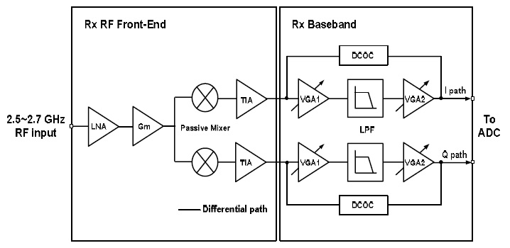
Fig. 1 shows a block diagram of the proposed zero-IF RF receiver, which consists of two parts: the RF front-end and the baseband circuit. The RF front-end is composed of a narrow-band low noise amplifier (LNA), a
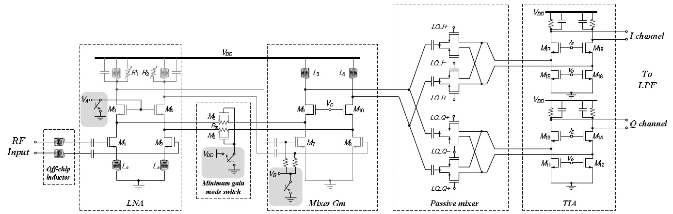
As shown in Fig. 2, the proposed LNA is a differential common-source amplifier with an inductive source degeneration to achieve a low noise characteristic and a high voltage gain versus power consumption. The LNA has an
In Fig. 2, the current-driven passive mixer architecture [5], which is composed of the
In the passive mixer, a trade-off between linearity and noise figure occurs directly, depending on the LO bias levels. In this work, the on-overlap LO biasing level has been chosen for the proposed passive mixer considering noise figure, conversion gain, and linearity.
The proposed TIA is a common-gate amplifier with low input impedance for the current-to-voltage conversion. It has the 1st-order
In order to ensure a wide dynamic range of the overall RF receiver, the gain of the RF front-end should be in the range of 41 to 23 dB with a step of 6 dB for the incoming input signal. The gain control from 41 to 29 dB has been achieved in the LNA load by adjusting the value of the resistors (
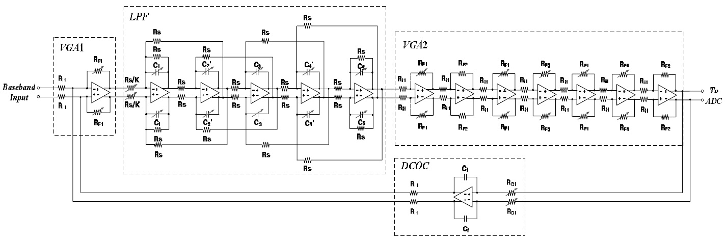
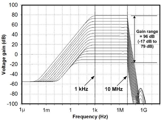
Fig. 3 shows the proposed analog baseband circuit (only I-path), comprising a VGA1, a channel-selection LPF, a VGA chain (VGA2), and a DCOC circuit. A lower noise figure of the receiver is achieved by locating the LPF between VGA1 and VGA2. The gain of the VGA1 suppresses noise from the LPF. The proposed analog baseband circuit provides a voltage gain from -23 to 79 dB in a 0.25 dB gain step.
In general, since active
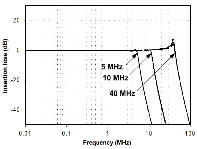
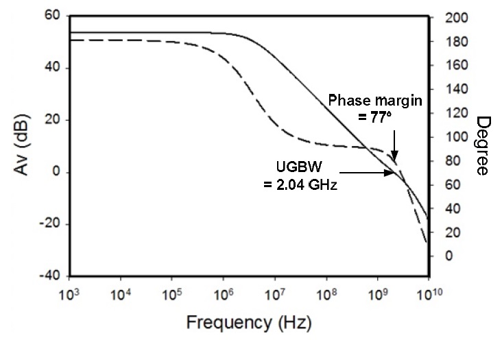
Fig. 4 shows the simulated frequency response of the proposed channel-selection LPF, where the cutoff frequencies of 5, 10, and 40MHz are not much changed for corner states of SS (-80℃), TT (27℃), and FF (40℃) mode. In Fig. 4, the peaking at 40MHz channel bandwidth comes from the deficient unit-gain bandwidth (UGBW) of 2.04 GHz in the proposed OP-amp. However, from the overall receiver measurements, the receiver does not show any oscillation problem or performances degradation.
The proposed VGAs (VGA1 and VGA2), which are composed of a fully differential OP-amp with a negative feedback resistor for high linearity, are designed to achieve -1 dB cutoff frequency of 50MHz for the maximum channel bandwidth of 40MHz [7].
In Fig. 3, the VGA1 provides a voltage gain from -12 to 12 dB with a 6 dB step. The VGA2 provides voltage gain from -11 to 67 dB with a 0.25 dB fine gain step to compensate I-Q gain mismatch. To provide the total gain of 67 dB, the VGA2 consists of 7 stages; the 1st, 3rd, and 5th amplifiers have a voltage gain from -12 to 12 dB with a 6 dB step respectively, the 2nd and 7th amplifiers provide a fixed voltage gain of 12 dB, the 4th amplifier provides a voltage gain from 1 to 6 dB with a 1 dB step, and the 6th amplifier provides a voltage gain from 0 to 1 dB with a 0.25 dB step.
A DCOC in a zero-IF receiver is inevitable, since an unexpected DC-offset may saturate the baseband output. The DC-offset problem is solved by building a DCOC loop based on voltage-current negative-feedback, as shown in Fig. 3. The high-pass cutoff frequency of the DCOC circuits is set to less than 1 kHz to ensure active sub-carriers around DC. However, due to this cutoff frequency of 1 kHz, the required capacitances
Fig. 5 shows the frequency response of the baseband circuit with a cutoff frequency of 10MHz. The baseband circuit provides a voltage gain from -23 to 79 dB, and the high pass cutoff frequency of less than 1 kHz. The simulated results of the proposed baseband circuit are summarized in Table 1.
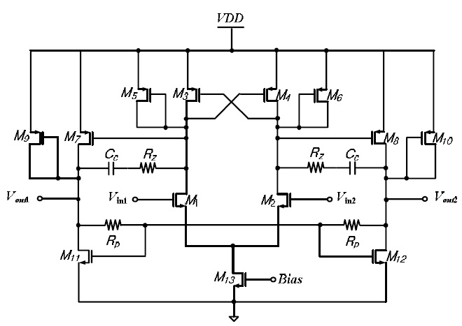
To achieve the channel bandwidth of up to 40MHz, the LPF and VGAs need a wideband OP-amp. Fig. 6 shows the proposed wideband two-stage OP-amp, which uses a crossconnected PMOS load (
[Table 1.] Performance summary of the baseband circuit
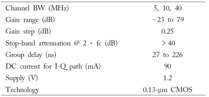
Performance summary of the baseband circuit
Fig. 7 shows simulated results of the proposed wideband OP-amp. The proposed OP-amp provides a phase margin 77° and a UGBW of 2.04 GHz, which is about 50 times the maximum channel bandwidth (40MHz). An OP-amp consumes 3.47 mA from a 1.2 V supply.
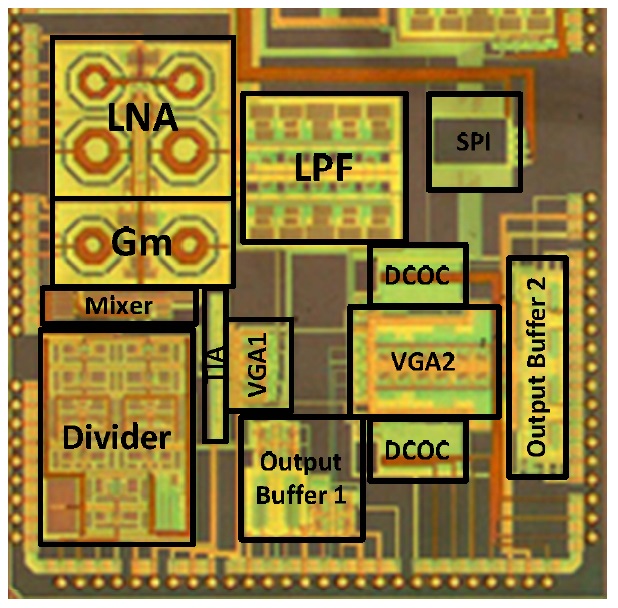
The proposed zero-IF CMOS RF receiver for LTE-Advanced systems has been implemented in 0.13-μm CMOS technology, as shown in Fig. 8. The receiver consumes 116 (high gain mode)/106 (low gain mode) mA from a 1.2 V supply.
Figs. 9-11 show the measured results of the fabricated chip. A 10-MHz 3G LTE signal only is applied to the input of the chip for measurements, even though the receiver supports multi-channels of 5, 10, and 40MHz.
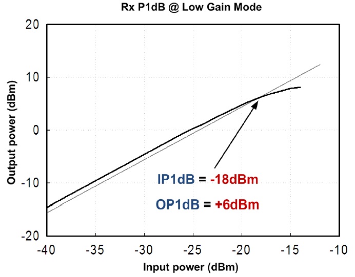
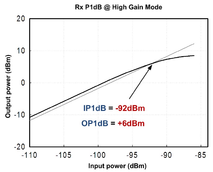
Figs. 9 and 10 show the measured an input 1- dB gain compression point (P1dB) of the proposed RF receiver with the high and low gain modes, respectively. Due to the sufficient linearity for all the signal paths, the proposed RF receiver achieves P1dB of -92 dBm (high gain mode) and -18 dBm (low gain mode) for a fixed output power of 6 dBm for 50 Ω loading. At the high and the low gain mode, a simulated overall gain of the RF receiver is 103/29 dB but the measurements show the 99/25 dB because of unexpected parasitic capacitances in the RF paths.
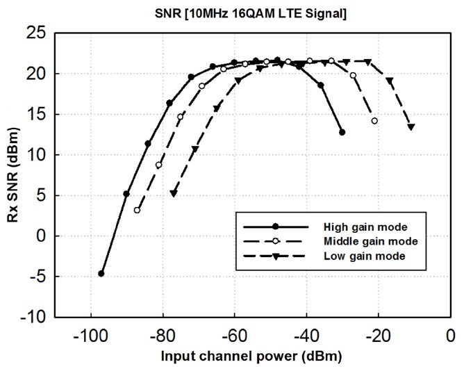
Fig. 11 shows the measured SNR for the 10-MHz 3G LTE input signal with 16-QAM. The proposed RF receiver provides more than 8.3 dB of minimum SNR [14], while receiving the input channel power from -88 to -12 dBm.
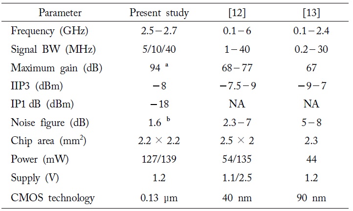
Table 2 summarizes the measured results and compares them with the state-of-the-art measurements [12,13]. The proposed RF receiver achieves the widest channel bandwidth, the highest gain, and the lowest noise figure.
This paper has presented a zero-IF CMOS RF receiver for LTE-Advanced systems, which is implemented in 0.13-μm CMOS technology. The simulated and the measurement results demonstrate that the proposed RF receiver can favorably support the LTE-Advance systems.
[Table 2.] Performance comparison

Performance comparison