Recently, the number of wireless communication services has been increasing steadily. With an ever-increasing number of frequency bands and diverse wireless communication standards, front-end complexity and costs have risen. Therefore, the conventional receiver architecture requires more chips. Consequently, a software-defined radio (SDR) receiver is needed to reduce complexity and costs [1]. An SDR receiver can accomplish this, but it can also suffer from outof-band interferences because it deals with wideband signals at the RF front-end [2].
Among various mixer architectures in SDR receivers, a hard-switching mixer is preferred, due to its superior gain and low noise characteristic [3,4].
However, the desired signal is aliased with the interferers which are located around local oscillator (LO) odd order harmonic frequencies when down-converted to the baseband at the hard-switching mixer stage. Multi-phase mixers have been suggested to suppress RF signals around LO harmonics [3,5,6]; however, they have the following drawbacks: 1) the seventh harmonic is not rejected and causes aliasing; 2) the third and fifth harmonic rejection (HR) performance is restricted by amplitude and phase mismatches; and 3) the complexity and size increase. The third HR ratio at the mixer stage is practically constrained to 30 to 40 dB, but much more rejection is needed to attenuate harmonic interferences with -40 to 0 dBm power down to the noise floor [7]. Therefore, a high HR ratio is required before the mixer stage.
In [8], a design technique is provided for high HR; however, this does not address the resistance of the inductor or the induced gate noise. In [9], the research also neglects these noise sources and the fabricated and measured results are not described. The present paper analyzes a high Q resonance technique with these noise sources and provides a design guideline.
In this paper, Section II discusses the high Q series resonance technique, while Section III describes the circuit implementation in detail. Section IV shows the experimental results of the demonstrated low-noise amplifier (LNA) circuit. Finally, a conclusion is given in Section V.
Ⅱ. THE HIGH Q SERIES RESONANCE TECHNIQUE
A MOSFET senses a voltage at the gate-source capacitor. Series resonance amplifies the in-band signal voltage and attenuates the out-band signal voltage at capacitor. Among the LNA architectures that use series resonance, the inductively degenerated LNA (L-CS LNA) [10] is popular and widely used. However, the voltage gain and HR are limited because the Q is constrained. A source degeneration technique simply provides input matching, although it decreases the Q.
Techniques for improving the Q of the LNA input passive network have previously been presented [8]. In [8], theoretically, a value of Q that can be obtained approximately two times larger than the L-CS LNA can be obtained when all parameters and conditions are same except input network. This is achieved by abandoning the degeneration inductor. However, an even higher Q is still needed to attain sufficiently high gain and a high HR ratio with low power operation. Moreover, this study did not consider the resistance of the inductor or the induced gate noise.
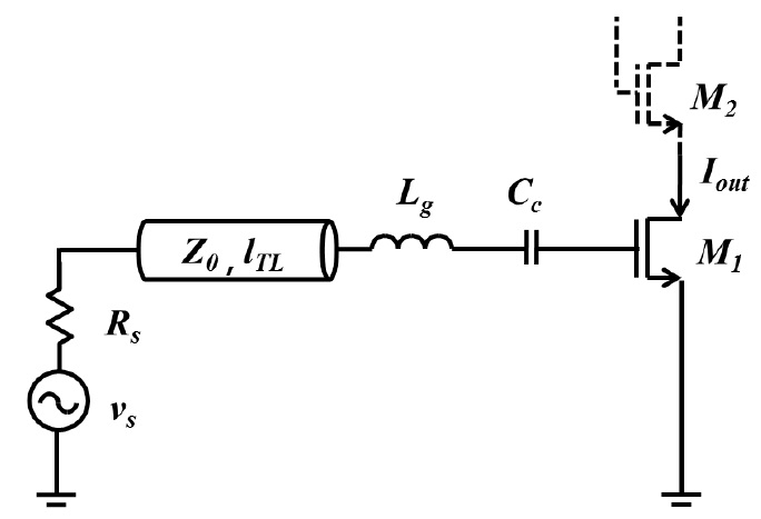
A high Q series resonance LNA (HQ-LNA) can overcome these problems, as shown in Fig. 1. A source impedance transformation provides higher Q resonance, as well as high gain and high HR. A source impedance transformation can be attained by a variety of methods, and a transmission line is a good approach. A multiband operation is also easily achieved by adjusting the resonance frequency, and this can be accomplished by changing the gate-source capacitor
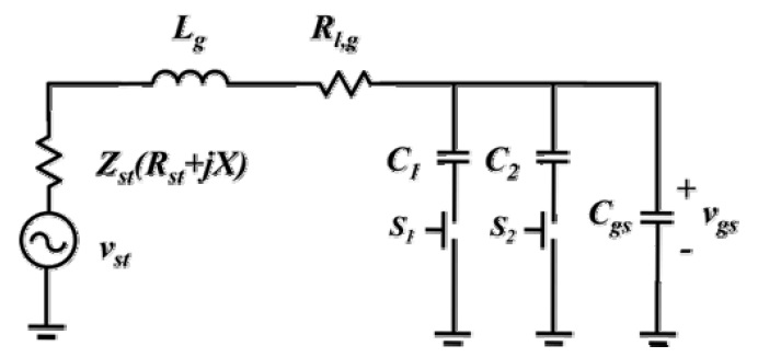
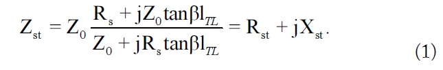
Fig. 2 shows the equivalent circuit of the proposed technique. The source voltage
The following analyses (gain and harmonic rejection ratio analysis) were performed with exclusion of the bonding effect. In this work, we minimized this effect by carried out multiple down bonding. Parasitic capacitances (routing parasitic capacitances, pad capacitances) also result in resistive input. If the bonding effect generates several tens of resistive impedance, then the effect must be included in the analysis. In that case, the
The transformed source impedance
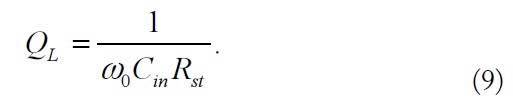
Therefore, the Q of the circuit can be written as:
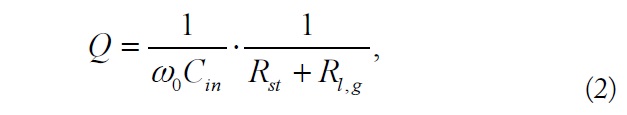
where ω0 is the series resonance frequency,
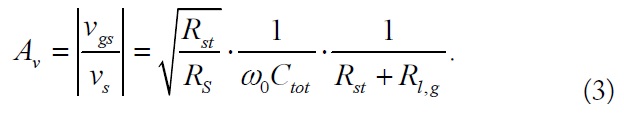
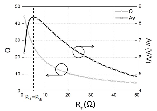
Fig. 3 shows that the Q and voltage gain are related to the resistance part of the source impedance.
The calculated Q and
and
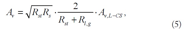
where
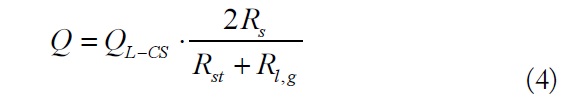
Eqs. (4) and (5) indicate that the HQ-LNA can have a much higher Q and voltage gain than the L-CS LNA if the source impedance
2. Harmonic Rejection Ratio Analysis
The third HR ratio can be calculated in a similar manner to the gain analysis. The third HR ratio is shown as:
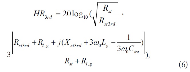
where
Gain and HR are important factors in an LNA. The derived equations show that gain is maximized when
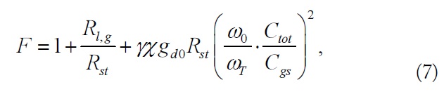
where
Here,
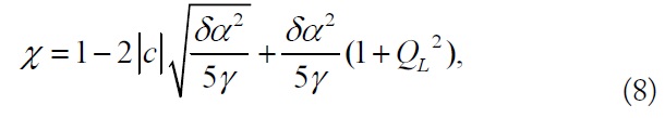
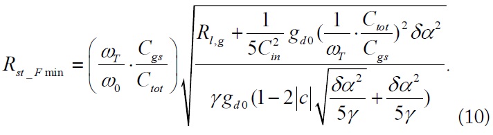
From (8), the optimum source impedance,
As the
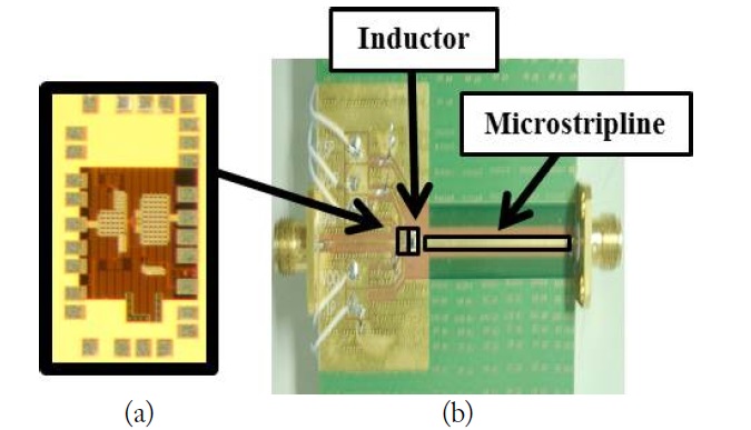
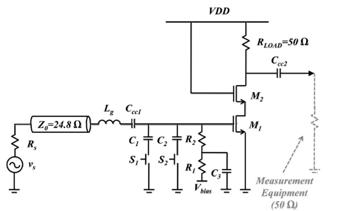
A HQ-LNA was designed and implemented using 0.13-μm CMOS technology, as shown in Figs. 4 and 5. The amplifiers had cascode configurations to improve the reverse isolation and reduce the Miller capacitance between the gate and the drain of the transistor,
Next, the proper transmission line was chosen. A 24.8-Ω characteristic impedance with 3.7 cm length line was selected to transform the source impedance,
The inductor,
Finally, the load stage was composed of only a 50 Ω resistor for measurement. This creates a low gain; however, it rarely contributes to the gain-frequency relation. Therefore, it will not interrupt the verification of the high Q resonance technique. In a practical case, the load stage can be composed of a wideband resonance circuit or high value resistor, and this provides more gain.
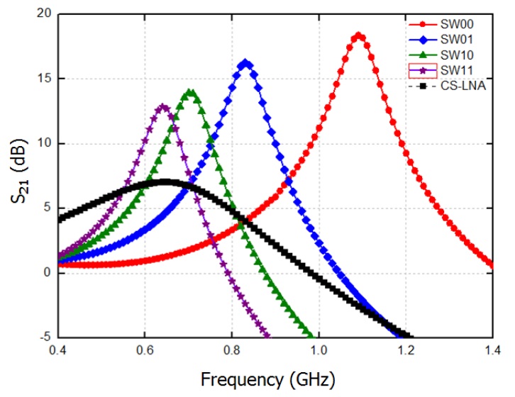
Fig. 6 and Table 1 show the simulation results for the HQ-LNA and the conventional L-CS LNA. They have the same architecture (cascade), same transistor size (width and length), same bias voltage (0.67 V), and same supply voltage (1.2 V); only the input matching part is different. The HQ-LNA SW11 mode is compared with the L-CS LNA, and the HQ-LNA exhibited higher gain, higher HR, and lower NF.
[Table 1.] The HQ-LNA and conventional L-CS LNA simulation results
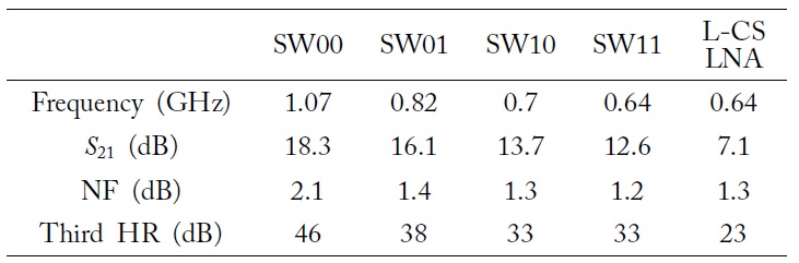
The HQ-LNA and conventional L-CS LNA simulation results
In the analysis, the
[Table 2.] Comparative summary about the frequency, NF, and third HR of LNAs
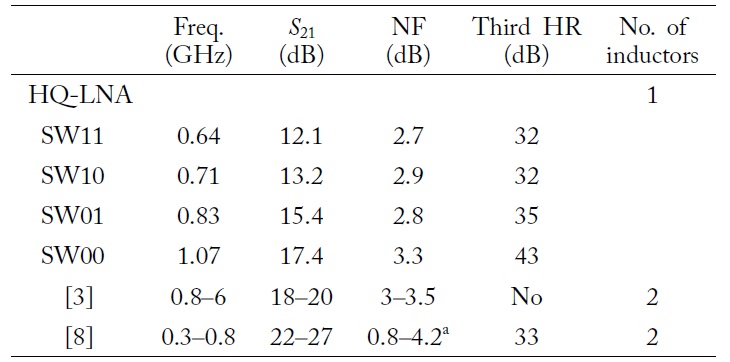
Comparative summary about the frequency, NF, and third HR of LNAs
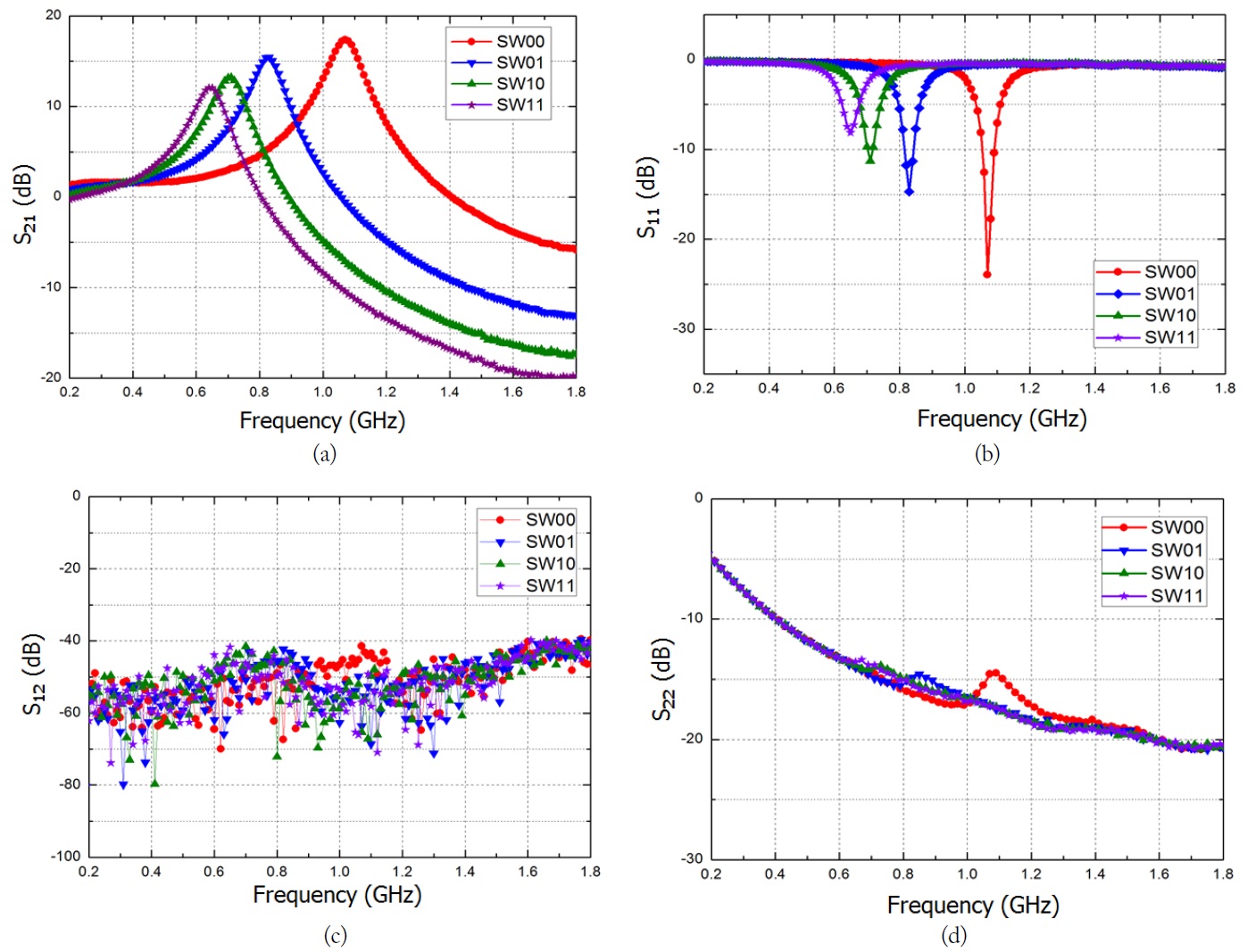
Fig. 7 shows the measured scattering (
Linearity was measured by two tone input signals, which are separated 1MHz from the center frequency at the upper and lower sides in each operating mode. The measured IIP3s were -5.7, -6.1, -8, and -10.8 dBm in the SW11, SW10, SW01, and SW00 modes, respectively.
For comparison, Table 2 gives a summary of the measured results of operation frequency, NF, and third HR for several LNAs. A wideband LNA in [3] does not provide third HR. The SW00 mode achieves the highest third HR ratio. HQ-LNA has slightly lower gain, due to it uses 130-nm CMOS process and load stage consists of pure 50 Ω resistor. This 50 Ω resistor load provides more precise observation about input network effects; however, it provides low gain. In practice, a load can consist of a resonance circuit or a higher resistor, and it can provide more gain.
In this paper, we presented a high Q input series resoance LNA to obtain high voltage gain, a high HR ratio, and low NF, as well as to support multiband operation for an SDR receiver. This technique was simply achieved by exploiting switchable capacitor banks, one inductor, and a transmission line. The high HR will relax the specification of the filter when using a hard-switching mixer.
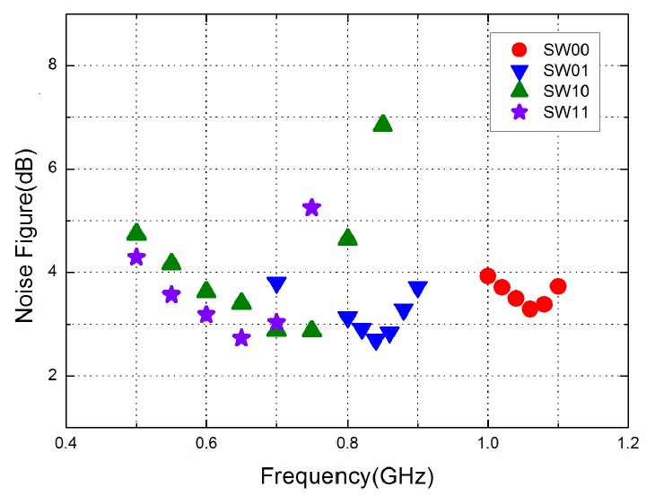
These effects were demonstrated by measurement of the implemented LNA. The LNA supports four operation bands (0.64, 0.71, 0.83, and 1.07 GHz) with high forward gain (12.1, 13.2, 15.4, and 17.4 dB), low NF (2.7, 2.9, 2.8, and 3.3 dB), high third HR ratios (32, 32, 35, and 43 dB), and low power consumption (9.6 mW with 1.2 V). The proposed technique is a promising option for high-performance, low-cost SDR receivers.