검색 전체 메뉴
PDF
맨 위로
OA 학술지
A New Design Approach for Asymmetric Coupled-Section Marchand Balun
  • 비영리 CC BY-NC
  • 비영리 CC BY-NC
ABSTRACT
A New Design Approach for Asymmetric Coupled-Section Marchand Balun
KEYWORD
Asymmetric Balun , Asymmetric Coupled Transmission Lines , Marchand Balun , Wideband.
  • Ⅰ. INTRODUCTION

    Due to compact configuration and ease of fabrication, the Marchand balun has been widely used since it was introduced [1-3]. As the operating frequencies for microwave and millimeter-wave systems increase, baluns composed of transmission lines have been integrated with amplifiers, mixers and frequency generators/converters since the balanced operation takes advantages over single-ended operation on various performances, such as noise reduction, power supply stability, and linearity, etc. [4-6]. MMICs are also now integrating this transmission line based baluns with active and passive circuits in single chip because transmission lines can be integrated conveniently for millimeter-wave frequencies. Therefore, more compact designs for baluns are continuously required for modern microwave and millimeter-wave systems.

    The Marchand balun has attracted substantial interest for performing this functionality because this balun can be constructed for very wideband and simple fabrication [7-10]. It is constituted generally using two identical symmetric coupled sections for simplifying the design. Since the symmetric coupled section is mainly characterized by the coupling factor, most of Marchand baluns composed of symmetric coupled sections are established using the design equation for the coupling factor according to design specifications [11-15]. In spite of its relatively easy implementation, Marchand baluns using symmetric coupled sections impose restriction on band extension and adjustability because very tight coupling is needed for wideband and not easy for fabrication. Asymmetric coupled-sections possibly using multilayer configuration may be employed for overcoming this restriction, however the design procedure will be more complicated compared with simple symmetric coupled section based Marchand baluns [16-18].

    Not depending upon the coupling coefficient, Marchand balun can also be designed using the procedure presented in [8] where several sets of design equations are derived and capitalized for designing the asymmetric coupled line based Marchand balun. Although [4] and [19] do not use the coupling coefficient, explicit expression for obtaining the design equations are not shown, but just providing available ranges for characteristic impedances of transmission lines located over multilayers. Therefore, it seems to be quite difficult to obtain the exact design parameters, leading to possibility to distracted design since only ranges for design parameters are given. It is highly desired that the design equations for obtaining circuit configuration be explicitly characterized and the design procedure be clearly defined for asymmetric coupled line based Marchand balun.

    In this work, a systematic design for achieving the characteristics of asymmetric coupled transmission lines over two layers is proposed for building the Marchand baluns. We do not use coupling coefficients for the asymmetric coupled lines, instead explicit expression for characteristic impedances is derived. Without using coupling coefficients, characteristic impedance of a transmission line on top layer over other wide transmission line located on bottom layer is derived using the balun requirements. The characteristic impedance of the transmission line on bottom layer can also be calculated assuming that this transmission line is so wide that this can be approximated to a single transmission line with ground layer located below this wide line. Other than characteristic impedances, electrical lengths for the coupled lines are also exploited for design parameters, which is not a general procedure for conventional design for Marchand baluns. In conventional design, electrical length is maintained to be 90°, however, electrical length can be varied for achieving the design specifications in this work, specially related to extending the bandwidth. Newly derived design equations are revealed in Section II, a Marchand balun is designed and evaluated according to the proposed procedure as explained in Section III, and finally conclusion is included in Section IV.

    Ⅱ. DESIGN PROCEDURE

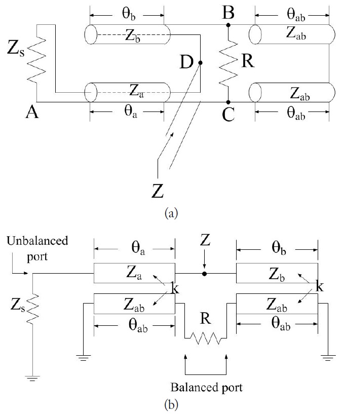
    The basic Marchand balun can be represented by using transmission lines as shown in Fig. 1(a) where unbalanced signal enters from A and balanced signal comes out between B and C. This type of balun can be equalized to the circuit as shown in Fig. 1(b) where two coupled sections are exploited for obtaining 3-dB insertion loss and coupling factor k determines the physical dimensions of the coupled sections.

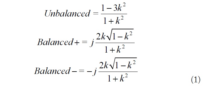
    For symmetric coupled sections, even- and odd-mode characteristic impedances are discovered, however, 3-dB coupling providing an overall 3-dB insertion loss for the coupled sections is so tight that this configuration shows a difficulty in obtaining acceptable insertion loss. Relative signal strengths coming into the unbalanced port and out of the balanced port are represented as in Eq. (1) where k is the coupling factor. As described in Eq. (1), only one solution is available for the coupling factor to achieve zero return loss and 3-dB insertion loss, and in some case unrealistic physical geometry is required.

    image
    image

    Due to this restriction, asymmetric coupled-sections over two layers may replace the symmetric coupled sections for realistic implementation of 3-dB insertion loss. Ambiguous design equation expressed in Eq. (2) has been needed conventionally for obtaining physical geometry of asymmetric coupled-sections as derived in [10]. However, Eq. (2) does not have to be satisfied if the proposed design approach here in this paper is capitalized as explained later. Since no design equations manifest themselves in explicit expression up to now, it is highly desirable that more obvious representation be derived.

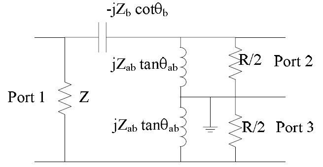
    The equivalent circuit for Fig. 1 looking into Z may be redrawn as shown in Fig. 2 where the original unbalanced port can be thought to be propagated back by amount of θa from Z [3]. Since the characteristics of balun can be understood mainly in terms of reflection coefficient at the unbalanced port (port 1) and transmission coefficients from unbalanced port to balanced port, three-port [S]-matrix is given as shown in Eq. (3),

    image

    To derive the explicit design equations for asymmetric coupled-line based Marchand balun, necessary
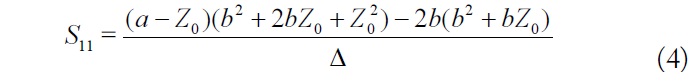
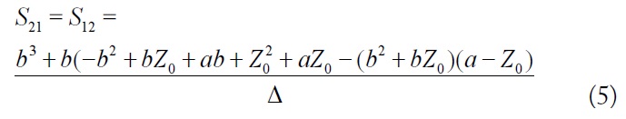
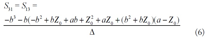
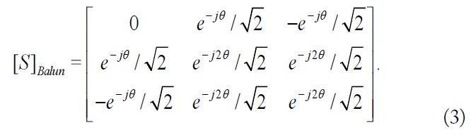
 S-parameters for the equivalent circuit as described in Fig. 2 are calculated for balun to work as represented in Eqs. (4)-(6) using a = j2zab tan θab - jZb cot θb and b = -jZb cot θb,

    image
    image
    image

    where Δ = -2b3 - b2Z0 + ab2 + 2bZ20 + 2abZ0 + Z30 + aZ20.

    From Eq. (3), S11 should be zero for this equivalent circuit to work as a balun, therefore real and imaginary parts of S11 are zero as deduced in Eqs. (7) and (8). Solving Eqs. (7) and (8), two explicit solutions are derived as seen in Eqs. (9) and (10).

    image
    image
    image
    image

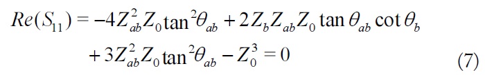
    Substituting Eqs. (9) and (10) into Eqs. (5) and (6), we can confirm that this equivalent circuit satisfies the requirement for balun to work since and leading to and ∠S21−∠S31 = 180°. Once Zb, Zab, θb, and θab are determined satisfying Eqs. (9) and (10), physical geometry for balun can be obtained using electromagnetic (EM) simulation programs. Za and θa do not affect balun equation, so that they can be equalized to Zb and θb, respectively. Since four parameters are to be determined (Zb, Zab, θb, and θab), two design freedoms for determining these parameters using Eqs. (9) and (10) are available. Rearranging Eqs. (9) and (10),

    image

    where 90° for θb and θab is excluded to determine Zb and Zab. In case of 90° both for θb and θab, the capacitance is shorted and inductances are open, resulting in S11 of 1/3 (= -9.5 dB). For Z0 = Zb = Zab, the perfect match occurs when θb = θab = 45°, 135°, 225°, etc., as drawn in Fig. 3 where the fractional bandwidth based on S11 of under -10 dB goes up to 116%. But for Zb or ZabZ0, θb and θab do not need to be same any more, yielding smaller bandwidth. For a maximum bandwidth, θb and θab should be maintained close to 90°.

    Once Zb and Zab are determined initially by considering physical implementation, θb and θab can be determined as close as possible to 90° by taking into account the desired bandwidth in terms of S11.

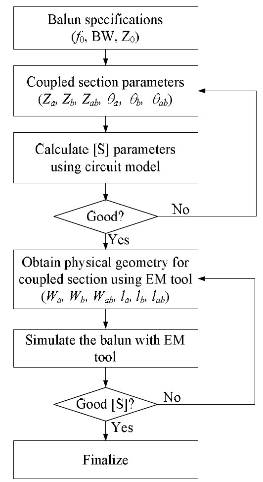
    A systematic procedure for designing asymmetric coupledline based Marchand balun is summarized in the flow diagram of Fig. 4 where two steps are used for arriving at the final physical geometry. At the first step, coupled section parameters are decided using Eqs. (9) and (10) from the desired balun specifications. These parameters constitute an equivalent circuit model as in Fig. 2, and S-parameters are calculated for verifying the coupled section parameters. At the second step, the calculated coupled section parameters are exploited to obtain the physical widths and lengths (Wa, Wb, Wab, la, lb, and lab) as exhibited in Fig. 4. Usually, Wa is set equal to Wb, and la = lb is used for simplifying the design. Extended lines with 50 Ω are added to line lab to connect ports 2 and 3 conveniently to this balun. Wa (= Wb) is obtained by regarding the wide transmission line located on bottom layer of Zab used as the reference layer, and Wab is obtained as a general transmission line located over a ground layer where narrow transmission line located on top layer is used for synthesizing Wab.

    The characteristic impedance (Zab) of wide line on bottom layer can be thought to be little deviated from that of a general transmission line since a very narrow line is located on top layer. Therefore, this assumption does not affect the characteristic impedance of wide transmission line on bottom layer.

    Ⅲ. DESIGN OF THE ASYMMETRIC MARCHAND BALUNS

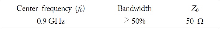
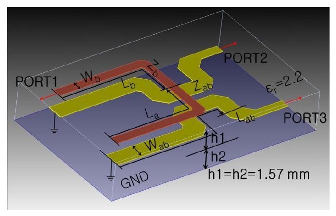
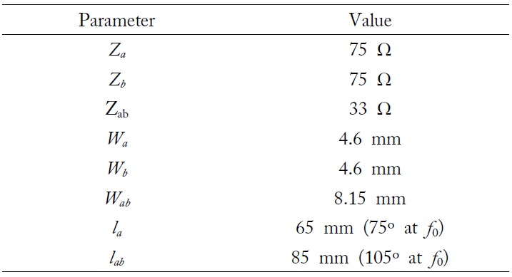
    Based on the design procedure developed in Section II, a balun using asymmetric coupled-sections over two layers is designed varying characteristic impedances as illustrated in Fig. 5. Desired specifications are chosen as listed in Table 1. Design parameters and physical geometries for the design example are achieved as illustrated in Table 2 where the electrical lengths (θa and θb) are initially set to 90° at the center frequency of 0.9 GHz as a design freedom. Using Figs. 2 and 3, θb = 75° and θab = 105° are then optimized with the pre-selected Zb = 75 Ω and Zab = 33 Ω. It is found that the relation between characteristic impedances is completely different from Eq. (2), therefore, a large number of freedoms in choosing design parameters are available.

    [Table 1.] Desired balun specifications

    label

    Desired balun specifications

    [Table 2.] Parameters for design example of asymmetric coupledsection based balun

    label

    Parameters for design example of asymmetric coupledsection based balun

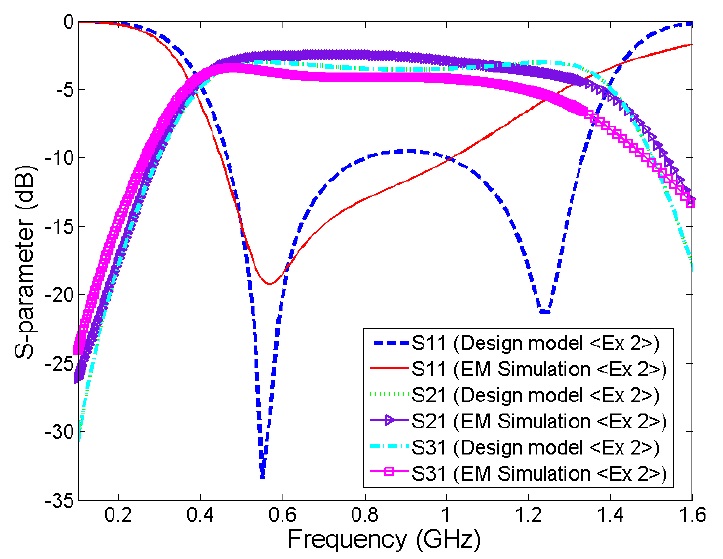
    Using the physical geometry obtained here, an asymmetric coupled-section based Marchand balun has been simulated on a full-wave EM simulator. S-parameters obtained from an EM simulator are displayed as shown in Fig. 6, and compared with those calculated from the equivalent circuit model as in Fig. 2. It is seen that the insertion loss is -3.2 to -2.5 dB, the amplitude imbalance is within 1.5 dB, and the phase imbalance is less than 5° over the frequency range of 0.5 to 1.0 GHz where |S11| is less than -10 dB. Although S11 obtained from an EM simulator shows disagreement in the higher frequency, S21 and S31 exhibit considerably outstanding result.

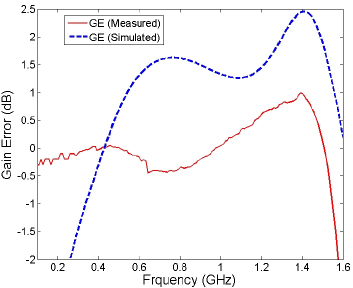
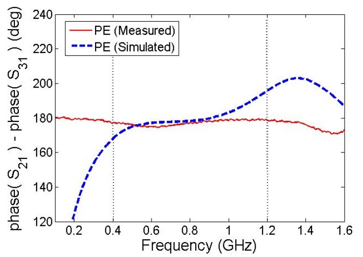
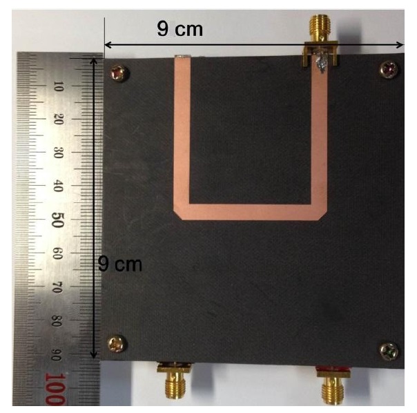
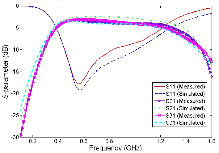
    The proposed balun using the layout depicted in Fig. 5 has been fabricated on Duroid 5880 substrate with dielectric constant of 2.2 and each layer thickness of 1.57 mm in two layer structure as shown in Fig. 6. Fig. 7 demonstrates S-parameter results from equivalent model and EM simulation. Deviation at the upper band is originated from the fact that Za and Zb used 75 Ω, resulting in some reflection with 50 Ω input (= ZS). Their S-parameters are measured and plotted in Fig. 8, |S11| is less than -10 dB over the frequency range of 0.43 to 1.0 GHz. The insertion losses are measured as -3.9 to -3.2 dB as in Fig. 8, the amplitude imbalances are measured less than 0.5 dB, and the phase imbalances are within 5° as shown in Figs. 9 and 10 (within vertically dashed lines), respectively. If 3-dB bandwidth is taken in terms of S21 and S31, the bandwidth is extended to 0.38 to 1.4GHz range which is around 1GHz bandwidth. These measurement results are in fairly good agreement with EM simulation results. Two factors affected the frequency response of this balun: 1) since Za of 75 Ω is used, S11 seen at port 1 is 0.2 (= -14 dB) at 0.9 GHz when Z is matched to 75 Ω, and S11 deviates away from this value as frequency goes up; 2) since the difference of Lab and La (or Lb) exists leading to significant effect at the high frequency, this yields degradation of S11 at higher frequency as shown in Figs. 8-10.

    The air gap between top and bottom layers has been fabricated and assembled to be kept very little. We watched measured performance by changing the intensity of tightening screws at the corners, but not much difference has been come up with.

    Ⅳ. SUMMARY

    A design approach for the asymmetric coupled-section based Marchand balun has been presented along with design equations. An equivalent circuit model is exploited for evaluating the initial balun design before synthesizing the physical layout. The analytical procedure provides explicit relation between characteristic impedances of couples sections instead of using coupling factor which has been widely used conventionally. Physical geometry for coupled section is achieved by synthesizing the characteristic impedance of coupled line through an EM simulator.

    This approach was validated by taking a design example for asymmetric coupled-section based Marchand balun. This balun was designed using two layers where unbalanced port is located on top layer, balanced port is located on bottom layer, and ground is underneath the bottom layer. One design was fabricated and measured to confirm the proposed design approach. Experimental results are compared with those from an EM simulator where both show good agreement as desired.

참고문헌
  • 1. Marchand N. 1944 “Transmission-line conversion transformers” [Electronics] Vol.17 P.142-145 google
  • 2. Dunn D. A., Mclaughlin J. W., Grow R. W. 1958 “A wide-band balun” [IRE Transactions on Microwave Theory and Techniques] Vol.6 P.314-316 google cross ref
  • 3. Oltman G. 1966 “The compensated balun” [IEEE Transactions on Microwave Theory and Techniques] Vol.14 P.112-119 google cross ref
  • 4. Chiou H. K., Yang T. Y. 2008 “Low-loss and broadband asymmetric broadside-coupled balun for mixer design in 0.18 μm CMOS technology” [IEEE Transactions on Microwave Theory and Techniques] Vol.56 P.835-848 google cross ref
  • 5. Mat D. A. A., Pokharel R. K., Sapawi R., Kanaya H., Yoshida K. 2011 “60 GHz-band on-chip Marchand balun designed on flat and patterned ground shields for millimeter-wave 0.18 μm CMOS technology” [in Proceedings of the Asia-Pacific Microwave Conference] P.884-887 google
  • 6. Tsai P. H., Lin Y. H., Kuo J. L., Tsai Z. M., Wang H. 2013 “Broadband balanced frequency doublers with fundamental rejection enhancement using a novel compensated marchand balun” [IEEE Transactions on Microwave Theory and Techniques] Vol.61 P.1913-1923 google cross ref
  • 7. Lan X., Fong F., Kintis M., Kono K., Yamauchi D., Luo W. B., Farkas D. 2010 “An ultra-wideband balun using multi-metal GaAs MMIC technology” [IEEE Microwave and Wireless Components Letters] Vol.20 P.474-476 google cross ref
  • 8. Liu J. X., Hsu C. Y., Chuang H. R., Chen C. Y. 2007 “A 60- GHz millimeter-wave CMOS Marchand balun” [in Proceedings of the IEEE Radio Frequency Integrated Circuits Symposium] P.445-448 google
  • 9. Chiang M. J., Wu H. S., Tzuang C. K. C. 2009 “A compact CMOS Marchand balun incorporating meandered multilayer edge-coupled transmission lines” [in Proceedings of the IEEE MTT-S International Microwave Symposium] P.125-128 google
  • 10. Govind V., Yun W., Sundaram V., Swaminathan M., Dalmia S., White G. 2005 “Analysis and design of compact wideband baluns on multilayer liquid crystalline polymer (LCP) based substrates” [in Proceedings of the IEEE MTT-S International Microwave Symposium] P.543-546 google
  • 11. Ng C. Y., Chongcheawchamnan M., Robertson I. D. 2002 “Analysis and design of a high-performance planar Marchand balun” [in Proceedings of the IEEE MTT-S International Microwave Symposium] P.113-116 google
  • 12. Ang K. S., Robertson I. D. 2001 “Analysis and design of impedance-transforming planar Marchand baluns” [IEEE Transactions on Microwave Theory and Techniques] Vol.49 P.402-406 google cross ref
  • 13. Lin C. S., Wu P. S., Yeh M. C., Fu J. S., Chang H. Y., Lin K. Y., Wang H. 2007 “Analysis of multiconductor coupled-line Marchand baluns for miniature MMIC design” [IEEE Transactions on Microwave Theory and Techniques] Vol.55 P.1190-1199 google cross ref
  • 14. Tang C. W., Cheng W. D., Wu J. W., Lin Y. C. 2010 “Design of a compact balun with three octant-wavelength coupled lines” [in Proceedings of the IEEE MTT-S International Microwave Symposium] P.109-112 google
  • 15. Ahn H. R., Nam S. 2011 “New design formulas for impedance-transforming 3-dB Marchand baluns” [IEEE Transactions on Microwave Theory and Techniques] Vol.59 P.2816-2823 google cross ref
  • 16. Schwindt R., Nguyen C. 1994 “Computer-aided analysis and design of a planar multilayer Marchand balun” [IEEE Transactions on Microwave Theory and Techniques] Vol.42 P.1429-1434 google cross ref
  • 17. Michaelsen R., Johansen T., Tamborg K., Zhurbenko V. 2013 “A modified Marchand balun configuration with tunable phase balance” [IEEE Microwave and Wireless Components Letters] Vol.23 P.66-68 google cross ref
  • 18. Tseng C. H., Hsiao Y. C. 2010 “A new broadband Marchand balun using slot-coupled microstrip lines” [IEEE Microwave and Wireless Components Letters] Vol.20 P.157-159 google cross ref
  • 19. Ma T. G., Cheng Y. T. 2009 “A miniaturized multilayered Marchand balun using coupled artificial transmission lines” [IEEE Microwave and Wireless Components Letters] Vol.19 P.446-448 google cross ref
OAK XML 통계
이미지 / 테이블
  • [ Fig. 1. ]  The conventional Marchand baluns using (a) Transmission lines and (b) coupled line sections.
    The conventional Marchand baluns using (a) Transmission lines and (b) coupled line sections.
  • [ Fig. 2. ]  Equivalent circuit for Marchand balun.
    Equivalent circuit for Marchand balun.
  • [ Fig. 3. ]  Calculated S11 (θ = θb = θab) using Fig. 2 with Z0 = Zb = Zab.
    Calculated S11 (θ = θb = θab) using Fig. 2 with Z0 = Zb = Zab.
  • [ Fig. 4. ]  A design approach for asymmetric coupled-section based Marchand balun.
    A design approach for asymmetric coupled-section based Marchand balun.
  • [ Table 1. ]  Desired balun specifications
    Desired balun specifications
  • [ Table 2. ]  Parameters for design example of asymmetric coupledsection based balun
    Parameters for design example of asymmetric coupledsection based balun
  • [ Fig. 5. ]  The physical layout of asymmetric coupled-section based Marchand balun.
    The physical layout of asymmetric coupled-section based Marchand balun.
  • [ Fig. 6. ]  The photograph of asymmetric coupled-section based Marchand balun.
    The photograph of asymmetric coupled-section based Marchand balun.
  • [ Fig. 7. ]  S-parameters from the equivalent model compared with electromagnetic (EM) simulation for a design example.
    S-parameters from the equivalent model compared with electromagnetic (EM) simulation for a design example.
  • [ Fig. 8. ]  The measured results of asymmetric coupled-section based Marchand balun.
    The measured results of asymmetric coupled-section based Marchand balun.
  • [ Fig. 9. ]  Amplitude imbalance of asymmetric coupled-section based Marchand balun. GE = gain error.
    Amplitude imbalance of asymmetric coupled-section based Marchand balun. GE = gain error.
  • [ Fig. 10. ]  Phase imbalance of asymmetric coupled-section based Marchand balun. PE = phase error.
    Phase imbalance of asymmetric coupled-section based Marchand balun. PE = phase error.
(우)06579 서울시 서초구 반포대로 201(반포동)
Tel. 02-537-6389 | Fax. 02-590-0571 | 문의 : oak2014@korea.kr
Copyright(c) National Library of Korea. All rights reserved.