검색 전체 메뉴
PDF
맨 위로
OA 학술지
Compact Dual-Band Three-Way Metamaterial Power-Divider with a Hybrid CRLH Phase-Shift Line
  • 비영리 CC BY-NC
  • 비영리 CC BY-NC
ABSTRACT
Compact Dual-Band Three-Way Metamaterial Power-Divider with a Hybrid CRLH Phase-Shift Line
KEYWORD
Delay Line , Dual-Band , Metamaterial , Phase-Shift Line , Power Divider , Size-Reduction.
  • Ⅰ. INTRODUCTION

    Every wireless communication system incorporates microwave power dividers, couplers, filters, and relevant parts [1-5]. In particular, since one path has to be branched (i.e., as found in an array antenna or comparator), the power divider is required at the junction between the route on one side and several ways on the other side. The rapid growth of the telecommunication industry has prompted microwave technologies to push the envelope to meet users’ demands, and power dividers have been developed to cope with the multiple bands for system integration, wide bands for broadband service, etc. [6,7]. While achievements have been made in diversified and upgraded functions of the radio-frequency (RF) equipment, the constraints placed on the physical size have become the developers’ main concern. The response to these design priorities has been to focus a great amount of research on the production of size-reduced advanced power dividers, created by bending and folding, cascaded multi- stages, grid array, slot coupling between layers, R-L-C loads, etc., without loss of generality [8-11].

    These conventional techniques, although prevalent, have the limitation of loss from multiple stages, restrictions in embedding a confined space, and higher cost due to stack-up fabrication. Alternative methods have been sought to iron out these problems, which have attracted substantial attention from the RF community [12-16]. For example, Caloz and Itoh [12] introduced composite right- and left-handed (CRLH) transmission lines; their attempts to realize the then-fancy phenomena of the backward wave, left-handed propagation, non-linear dispersion, and zeroth order resonance (ZOR) resulted in a long periodic geometry that comprised 24 cells of distributed elements [12]. They successfully demonstrated its metamaterial characteristics, but this geometry was too large for incorporation into a device. Hence, many cells of lumped elements were cascaded in series to generate +90° or -90° and were attached to the arms of couplers and power dividers. Similarly, Marques et al. [13] formed a pair of slot rings under each of the arms of the Wilkinson power divider for the purpose of reducing the overall size. Inoue et al. [14] introduced an LTCC CRLH-type component similar to the lumped element-based multiple cells. A printed and small power divider with a metamaterial-inspired T-junction was shown by Saenz et al. [15], but it lacked a theoretical aspect, and its applicability to current challenges is doubted.

    This paper proposes an improved method for fabrication of a smaller and more advanced component that will overcome the drawbacks of earlier metamaterial and ordinary approaches. A novel three-way dual-band CRLH power divider is designed to have a very small footprint and the equal power division and in-phase outputs. Differing from [16], a CRLH and short three-way dual-band power dividing structure is presented that provides a dual-band phase-error correction line. The solution process starts from the separate implementation of the 2:1 unequal and 1:1 equal power dividing blocks that are fully printed and metamaterials. This is followed by plugging the inputs of the equal block into an output of the unequal block for an initial 1:1:1 power divider, and slightly tuning the interconnection segment. This initial configuration and its possible modification inevitably give rise to phase errors between the outputs. Hence, we need a phase compensation line that works for the dual-band objective, but this is difficult to obtain only with the ordinary delay line for the single band or its harmonic relations. The dual-band phase compensation is accomplished by a hybrid CRLH phase-shift line as a mixture of the distributed and lumped elements, for the sake of efficiency and convenience. The design method is validated by evaluating the proposed metamaterial structure by circuit analysis and full-wave simulation in the solution process. This novel 1:1:1 power divider is manufactured through a low-cost fabrication with an inexpensive cheap substrate and its performance is measured to confirm its desirable power division ratio and equalized phases at the output ports, especially considering that its physical placement is friendly to RF system layouts. Its size-reduction effect and technical applicability are also addressed.

    Ⅱ. THE PROPOSED CIRCUIT CONFIGURATION AND DESIGN OF ELEMENTARY BLOCKS

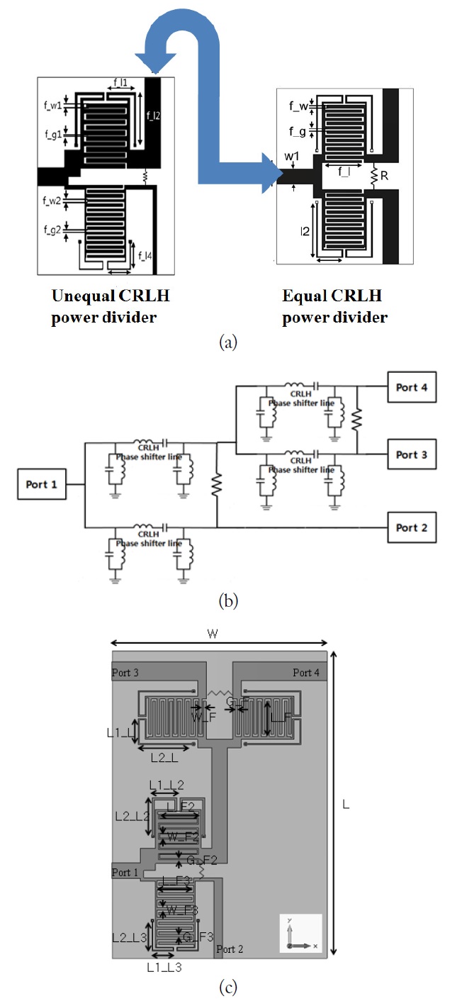
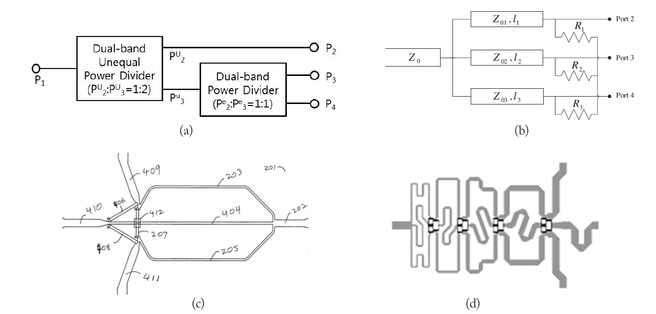
    A novel, compact three-way power divider with CRLH characteristics is schematized in the following figure and compared to three examples that used other techniques.

    Fig. 1(a) shows the composition of the proposed structure. The unequal power divider block is sequentially combined with the equal block, and both blocks are realized as printed CRLH devices with small footprints. Fig. 1(b) is an extension of the Wilkinson power divider to three ways, but has a single band. Elongated segments are added to the first stage in Fig. 1(c), and four stages are placed in chain in Fig. 1(d). Fig. 1(b)-(d) heavily depend on the quarter-wave long arm for each stage, with extra delay lines, but fail to achieve effective size-reduction. However, since a dual-band CRLH phase-shift line will be substituted for the single-band and quarter-wave long arms of the traditional Wilkinson power divider, Fig. 1(a) will be appropriate for the present objective.

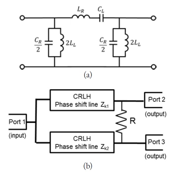
    The equivalent circuit of the aforementioned phase-shift lines for the dual-band unequal and equal power divider blocks shown in Fig. 1(a) is set up as follows.

    Fig 2(a) is used to create phase Φ1 for a lower frequency f1 and phase Φ2 for a higher frequency f2, where the ratio of f2 to f1 is arbitrary due to the occurrence of the non-linear dispersion curve. These phases and frequencies yield simultaneous equations containing the circuit elements, and mathematical manipulation renders L’s and C’s as given in the equations [16].

    image

    where ω1 = 2πf1 and ω2 = 2πf2, and Zc becomes Zk1 for one path and Zk2 for another path in an unequal power divider. In the present case, applying Φ1 = +90° at f1 = 960 MHz and Φ2 = -90° at f2 = 2.4 GHz to Eq. (1) for Fig. 2(a) results in the CRLH phase-shift line of the following data.

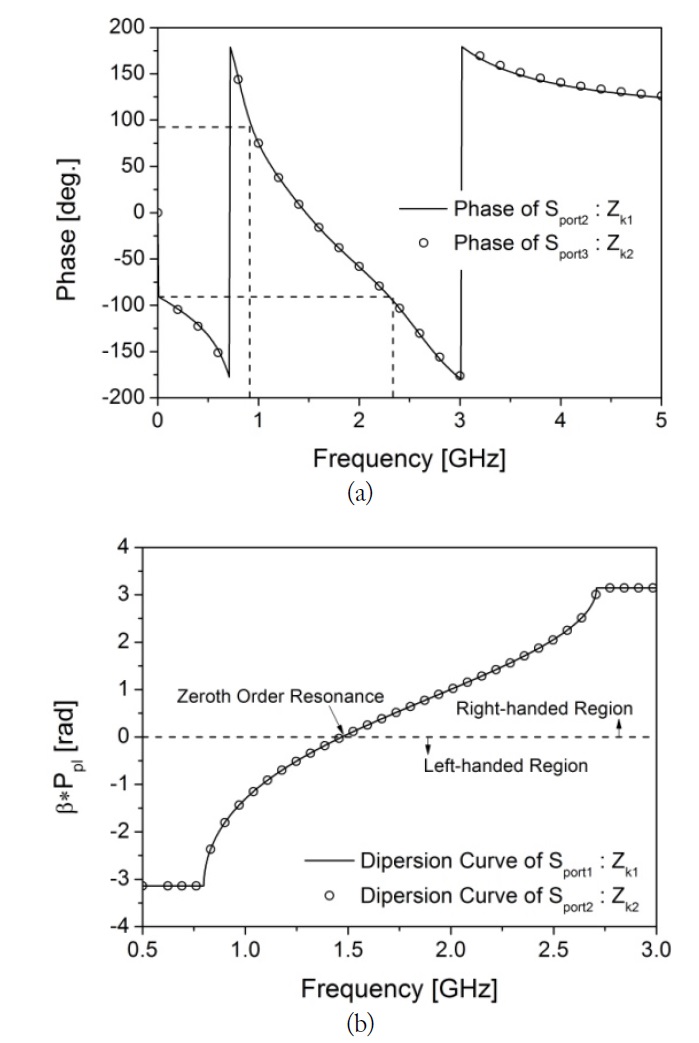
    Fig. 3(a) shows the phase as desired after applying Φ1 = +90° at f1 = 960 MHz and Φ2 = -90° at f2 = 2.4 GHz. This implies that this CRLH phase-shift line can be substituted for the quarter-wave long arms for the dual-band performance. Fig. 3(b) of the dispersion diagram presents the LH region including f1, the ZOR, and the RH region including f2 as a metamaterial property. This phase-shift line is input into the upper and lower paths of the dual-band unequal power divider as shown in Fig. 2(b). The characteristic impedance for each path is obtained with the following formulae, once we decide upon the power division ratio.

    image

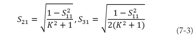
    Keeping in mind the connection to the equal block afterwards (to make the three-way power divider), the present unequal block should have the power division ratio of 2:1 with Zk1 = 51.5 Ω and Zk2 = 103 Ω. These impedance values are input into Eq. (1) with the previously mentioned phases, and the circuit elements of the phase-shift lines for both the paths are determined: CR, CL, LR, and LL are 4.7 pF, 2.0 pF, 5.9 nH, 2.5 nH in the 51.5-Ω path, and CR, CL, LR, and LL are 2.4 pF, 1.0 pF, 11.8 nH, 5.0 nH in the 103-Ω path. These lead to Fig. 3, in fact. The frequency response of the overall unequal block in Fig. 2(b), taking into account the CRLH phase-shift lines of Fig. 3, is observed by adopting the upcoming even- and odd-mode analysis techniques.

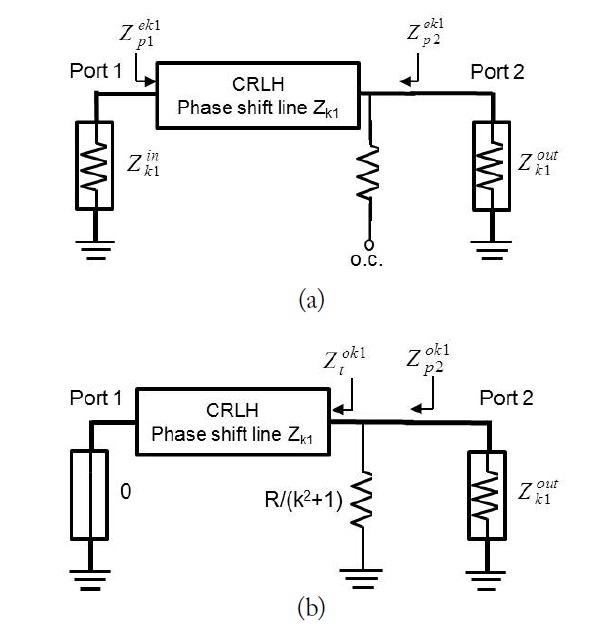
    Fig. 4(a) comes from Fig. 2, as ports 2 and 3 are excited with the in-phase signals and the bi-section line is treated as an open-circuited state. Fig. 2 becomes Fig. 4(b), in the assumption that the out-of-phase signals are fed into ports 2 and 3, and the axis of anti-symmetry is considered short-circuited. This applies to both the impedance lines. The frequency response of Fig. 2(b) will be given in the form of S-parameters, and the Z-parameters should be arranged for Fig. 2(a) and Fig. 4 in the first place. The series and shunt resonators in Fig. 2(a) are

    image

    With these, the diagonal and off-diagonal elements of the Z-parameter matrix for the CRLH phase-shift line can be written as

    image

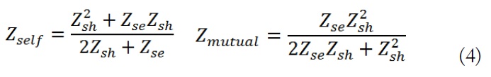
    The input impedance of the CRLH phase-shift line (the box in Fig. 4) is then obtained as
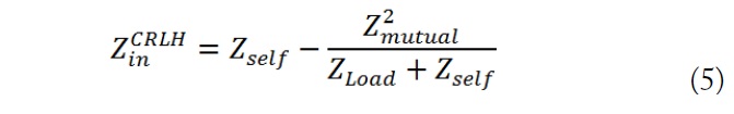
    image

    ZeK1p1 simply equals Eq. (5) in the even-mode, as in Fig. 4. Simultaneously, in the odd-mode case, the input impedance into the CRLH phase-shift line through Rk1 from the output port becomes

    image

    where Rk1 means R/(k2+1).

    For the equal block, Zk1 (= Zk2 = ZC) becomes 70.7 Ω.

    As long as the impedance matrix is completed, the corresponding S-parameters can be expressed as follows.

    image
    image
    image

    All the necessary S-parameters are described mathematically on the basis of the primary Z-parameters from Fig. 4 and the secondary ones of Eqs. (3)-(6). This process works for the unequal block, and also for the equal one. Therefore, the S-parameters are plotted as the frequency responses of the unequal and equal dual-band power dividers.

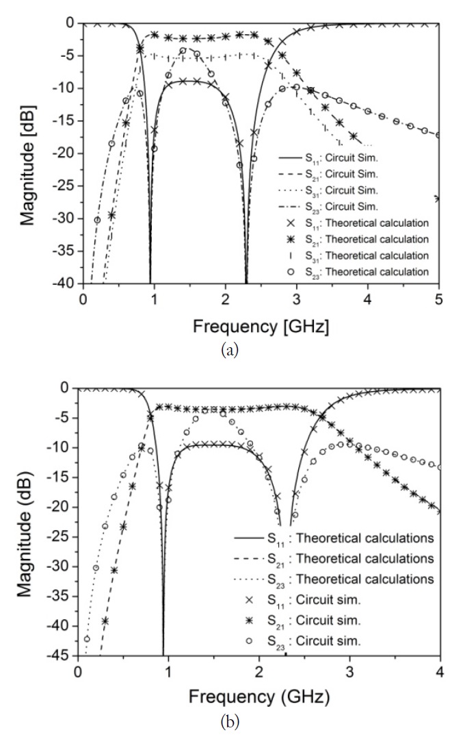
    The predicted performance of the 2:1 unequal power divider is shown in Fig. 5(a), where |S21| is -4.7 dB and -1.7 dB at 960 MHz and 2.4 GHz, as desired. |S21| is equal to |S31|, and the result of our code for the derived equations overlaps that of the commercial circuit analysis tool. Likewise, Fig. 5(b) shows a perfect agreement between the coding and the commercial program, and |S21| = -3 dB and |S31| = -3 dB as the 1:1 power division at the two target frequencies. The mathematical derivation has been validated and these elementary blocks are incorporated for the 1:1:1 power division.

    Ⅲ. THREE-WAY DUAL-BAND POWER DIVIDER BY COMBINING THE TWO BLOCKS AND PHASE CORRECTION BY A HYBRID CRLH LINE

    In this section, the unequal and equal blocks are interconnected to form the three equal outputs, and realized and tested in a full-wave simulation. One output is different from the remaining outputs in terms of phase for each of the two frequencies; therefore, the phase correction will be attained in an efficient way.

    The unequal and equal power-dividing circuits of Figs. 4 and 5 are physically implemented by following the steps of [16] to consider full-printing, and the input of the equal block is fed by the output of the 103-Ω path of the unequal dual-band power divider.

    Fig. 6(a) and (b) illustrate how to connect the unequal dual-band power divider to the equal block. In accordance with this scenario, the initial shape of the fully printed CRLH three-way dual-band power divider is presented as in Fig. 6(c). The geometrical parameters of the two blocks remain almost unchanged from those of the structure of the 1:1:1 power-divider except for the addition of the connecting part: W, L1_L, W_F, L_F, L2_L2, G_F2, L1_L3, W_F3, L_F3, L, L2_L, G_F, L1_L2, W_F2, L_F2, L2_L3, and G_F3 in Fig. 6(c) are 30.6, 3.5, 0.4, 5, 5.3, 0.1, 3.1, 0.4, 5, 43.7, 7.5, 0.2, 3.5, 0.6, 5.6, 4.1, and 0.3 mm, respectively, with FR4 of εr = 4.4 as the substrate. The guided wavelength of 960 MHz called λg requires the lengths of the CRLH phaseshift lines for the 51.5, 103, and 70.7 Ω paths to be 0.038 λg, 0.031 λg, and 0.034 λg in that order, which must be much less than 0.25 λg of one Wilkinson’s stage. The electrical size of the total foot print of Fig. 6(c) is estimated as 0.173 λg×0.247 λg, and its implication is a significant size-reduction effect compared with the Wilkinson’s power divider for the single band and its multi-stage applications for the dual-band operation. The performance is presented with the following figures.

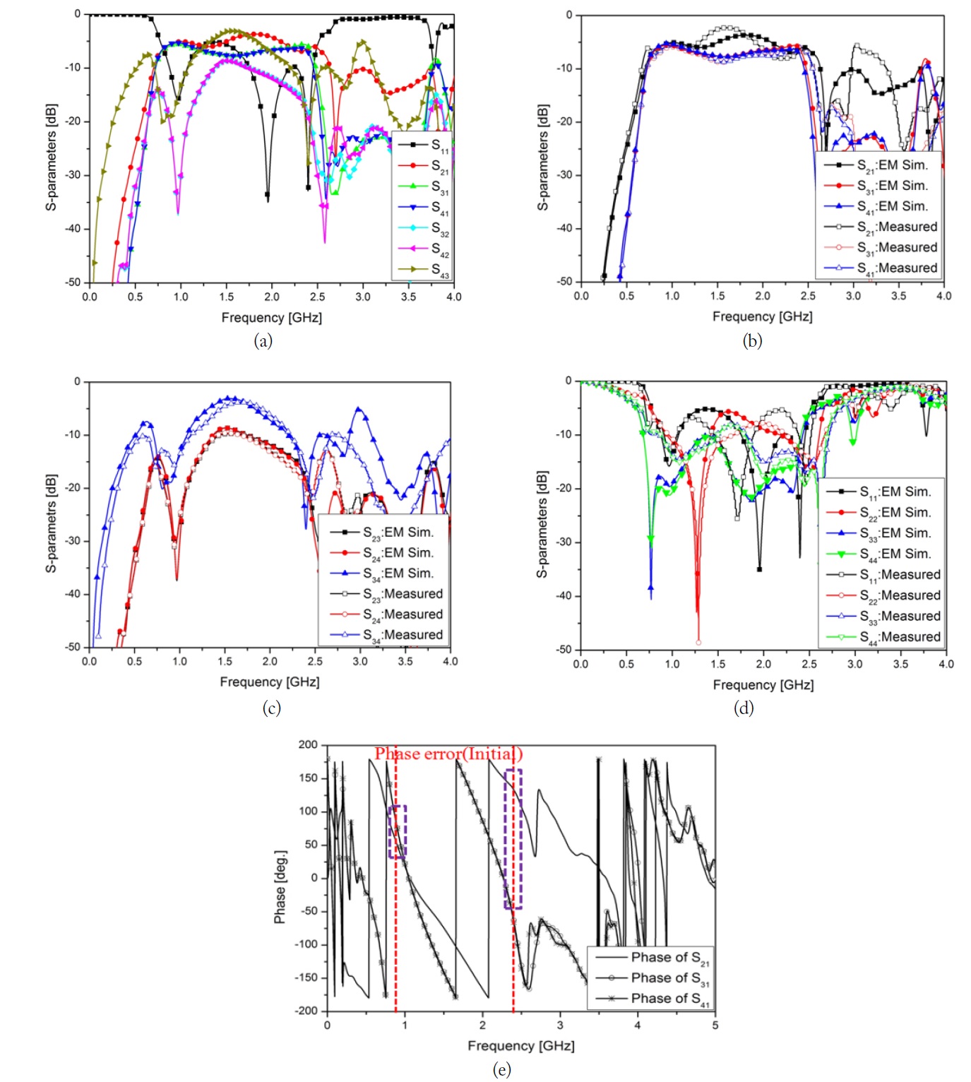
    In Fig. 7(a) and (b), equal power division to the 3 output ports is achieved with nearly -6 dB of |S21|, |S31|, and |S41| at 960 MHz and 2.4 GHz, simultaneously in the electro-magnetic (EM) simulation and measurement. Fig. 7(c) and (d) have |S23|, |S24|, and |S34|, and |Sii| below -12 dB at f1 and f2, more or less. Nonetheless, while the phases of S31 and S41 are the same, they differ from the phase of S21 as marked in Fig. 7(e). This causes the loss of a benefit of the in-phase outputs of the standard power divider. The location of port 2 in Fig. 6 also looks neither natural nor adaptable to RF cabling and harnessing. Therefore, the phase discrepancy with different values at 960 MHz and 2.4 GHz should be fixed by considering a change in the position of port 2. The fact that port 2 is located on the opposite side of ports 3 and 4, and off the extension line from port 1 in Fig. 6(b) means that it can be made friendly to the system cabling and integration by moving it to the same side as port 4, as an optimal choice. Assuming this positioning plan for port 2, we need to assign a box and fill it with a device to compensate for the different phase errors at 960 MHz and 2.4 GHz. Before solving this problem, the phase errors at the two frequencies with regard to a new location of port 2 should be checked. The changed layout differs from Fig. 7(e) and is given below. If a line shorter than 39 mm is chosen for the connection box, the phase errors will be known, given the layout of the modified three-way power divider, as follows.

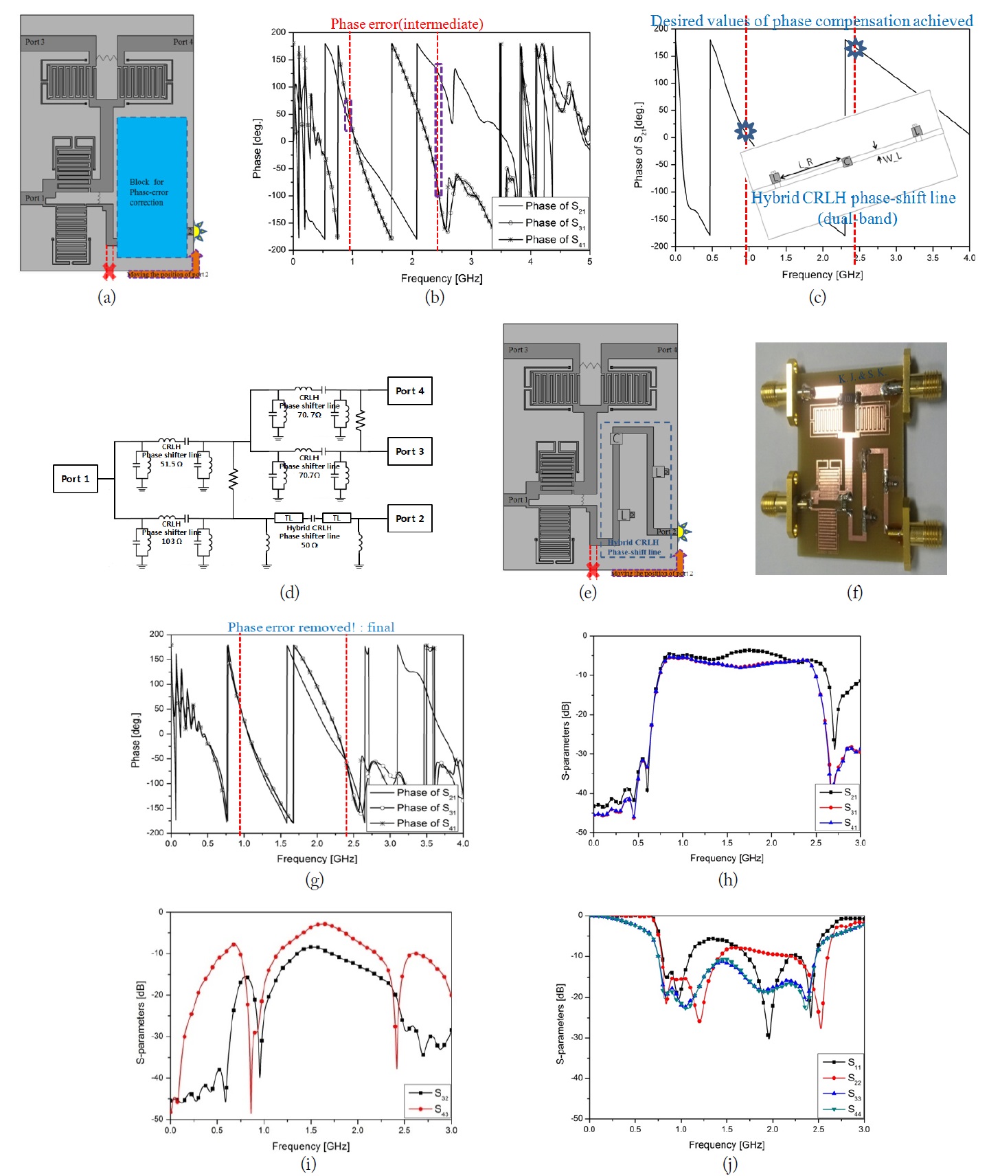
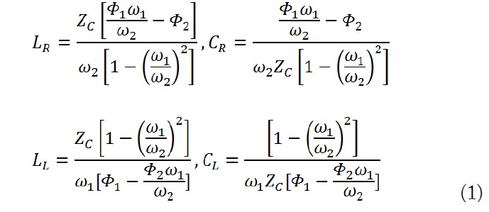
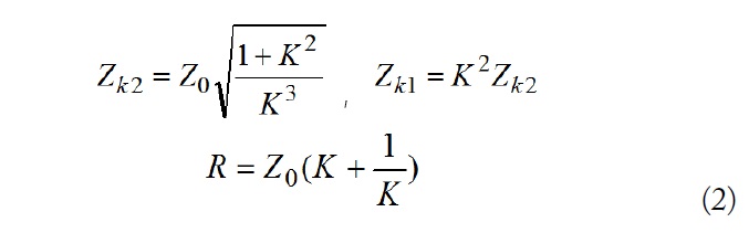
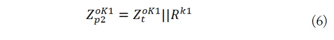
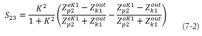
    The old port 2 in Fig. 7(e) is relocated, as shown in Fig. 8(a). A test line is inserted in the box to connect the output of the 103-Ω path of the unequal block to the new port 2, and the phase errors (Φ1 and Φ2) between S21 and S31 at f1 and f2 are found 14.5° and 168°, as observed in Fig. 8(b). A compact dual-band phase-shift line for Φ1 and Φ2 is made by a hybrid CRLH structure comprising a distributed element as the RH segment and lumped elements as the LH segment, as shown in the inset of Fig. 8(c)-Fig. 8(f). The RH segment is realized by a transmission line with L_R and W_L, while the two short-circuited chips L and the series chip C are responsible for the LH segment. Following the procedures to determine L and C as the unequal and equal block realization using Eq. (1), L_R, W_L, L, and C for Fig. 8(c)-Fig. 8(f) are calculated as 15 mm, 1.2 mm, 11 nH, and 1 pF, respectively, along with the following formulae regarding the RH segment.

    image

    where w, t, and h mean the width and thickness of the metal signal trace, and the height of the microstrip-line substrate, in that order. This dual-band hybrid CRLH phase-shift line attains Φ1 at f1 and Φ2 at f2 as desired, and it is presented by the measured data in Fig. 8(c). Consequently, the phase errors of Fig. 8(d) and (e) are corrected, and the identical phases at the three output ports are accomplished as in Fig. 8(f). Its area is kept the same as 0.173λg × 0.247λg, which validates the miniaturization effect of the proposed scheme. The magnitudes of the S-parameters of this final geometry are also plotted in Fig. 8(h)-Fig. 8(j). The equal power division is achieved at the three output ports, although an insertion loss of around -0.5 dB from the ideal power of -4.7 dB occurs due to the accumulated dielectric loss of FR4 and the conduction loss of copper. The inter-port isolation is observed below -15 dB at f1 and f2. In addition, a good impedance match is apparent at the ports, with a return loss below -15 dB at the two target frequencies. Lastly, the restriction of the ordinary delay line to meet only either Φ1 or Φ2 is described.

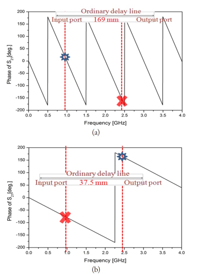
    The ordinary delay line is not able to achieve Φ1 and Φ2 at the target frequencies. The conventional delay line has the phase of a linear function; therefore, it works for a single band and its harmonics. In Fig. 9(a), the 169-mm long delay line can make 14.5° at f1, but fails to create Φ2 at f2. In addition, a line of this length will also exceed the footprint of the proposed three-way power divider. The use of the 37.5-mm long delay line also only satisfies 168° at f2, but is forbidden at f1 for Φ1. Therefore, our CRLH power divider outdoes the conventional components in that it results in a small size, but retains equal power division and inphase outputs based on the non-linear dispersion properties.

    Ⅳ. CONCLUSION

    This paper proposes a small sized three-way power divider with a 1:1:1 power division and in-phase outputs to work for two frequencies. It consists of 2:1 unequal and equal dual-band power dividers that are fully printed CRLH building blocks and incorporated to make a compact device to divide one RF input power into three ways. In particular, the phase errors between port 2 and ports 3 or 4 at 960 MHz and 2.4 GHz are observed in the initial three-way power divider, and they have been compensated for to equalize the output phases by designing a hybrid CRLH dual-band phase-shift line. The suggested method is shown to be valid through circuit analysis based on the derived equations, a full-wave simulation, and the measurement of the fabricated prototype. The overall size is much less than that of Wilkinson and modified power dividers. This method is applicable to the designs of advanced power dividers.

참고문헌
  • 1. Pozar D. M. 1998 Microwave Engineering google
  • 2. Wu Y., Zhou H., Zhang Y., Liu Y. 2008 "An unequal Wilkinson power divider for a frequency and its first harmonic" [IEEE Microwave and Wireless Components Letters] Vol.18 P.737-739 google cross ref
  • 3. Wu Y., Liu Y., Zhang Y., Gao J., Zhou H. 2009 "A dual band unequal Wilkinson power divider without reactive components" [IEEE Transactions on Microwave Theory and Techniques] Vol.57 P.216-222 google cross ref
  • 4. Cheng K., Li P. 2009 "Novel power divider design with unequal power-dividing ratio and simple layout" [IEEE Transactions on Microwave Theory and Techniques] Vol.57 P.1589-1594 google cross ref
  • 5. Sun Z., Zhang L., Yan Y., Yang H. 2011 "Design of unequal dual band Gysel power divider with arbitrary termination resistance" [IEEE Transactions on Microwave Theory and Techniques] Vol.59 P.1955-1962 google cross ref
  • 6. Oraizi H., Sharifi A. R. 2011 "Optimum design of asymmetrical multisection two-way power dividers with arbitrary power division and impedance matching" [IEEE Transactions on Microwave Theory and Techniques] Vol.59 P.1478-1490 google cross ref
  • 7. Sakagami I., Wuren T. 2009 "Compact multi-way power dividers for dual-band, wide band and easy fabrication" [in Proceedings of the IEEE Microwave Symposium Digest] P.489-492 google
  • 8. Srisathit S., Virunphun S., Bandudej K., Chongch-eawchamnan M., Worapishet A. 2003 "A dual-band 3-dB three-port power divider based on a two-section transmission line transformer" [in Proceedings of the IEEE Microwave Symposium Digest] P.35-38 google
  • 9. Wu L., Sun Z., Yilmaz H., Berroth M. 2006 "A dualfrequency Wilkinson power divider" [IEEE Transactions on Microwave Theory and Techniques] Vol.54 P.278-284 google cross ref
  • 10. Kawai T., Nakashima Y., Kokubo Y., Ohta I. 2008 "Dualband Wilkinson power dividers using a series RLC circuit" [IEICE Transactions on Electronics] Vol.91C P.1793-1797 google cross ref
  • 11. Wang D., Tang W., Xu X. 2008 "Isolation characteristics of microstrip Wilkinson dual-band power divider" [in Proceedings of the Asia-Pacific Microwave Conference] P.1-4 google
  • 12. Caloz C., Itoh T. 2006 Electromagnetic Metamaterials: Transmission Line Theory and Microwave Application. google
  • 13. Marques R., Martin F., Sorolla M. 2008 Metamaterials with Negative Parameters: Theory, Design and Microwave Applications. google
  • 14. Inoue N., Kawakami T., Horii Y., Kitamura T. 2010 "A super-compact dual-band Wilkinson power divider composed of multi-layered CRLH transmission lines" [in Proceedings of the 40th European Microwave Conference] P.433-436 google
  • 15. Saenz E., Cantora A., Ederra I., Gonzalo R., de Maagt P. 2007 "A metamaterial T-junction power divider" [IEEE Microwave and Wireless Components Letters] Vol.17 P.172-174 google cross ref
  • 16. Eom D. J., Kahng S. 2013 "Fully printed dual-band power divider miniaturized by CRLH phase-shift lines" [ETRI Journal] Vol.35 P.150-153 google cross ref
OAK XML 통계
이미지 / 테이블
  • [ Fig. 1. ]  The topological or structural differences between the proposed and other power dividers. (a) Topology of the proposed power divider, (b) expanded Wilkinson, (c) United States Patent 7164903, and (d) a product of InStock Wireless Components, Inc.
    The topological or structural differences between the proposed and other power dividers. (a) Topology of the proposed power divider, (b) expanded Wilkinson, (c) United States Patent 7164903, and (d) a product of InStock Wireless Components, Inc.
  • [ Fig. 2. ]  The equivalent circuits of the composite right- and lefthanded (CRLH) phase-shift line (a) and the unequal power divider (b).
    The equivalent circuits of the composite right- and lefthanded (CRLH) phase-shift line (a) and the unequal power divider (b).
  • [ Fig. 3. ]  The characteristics of the composite right- and left-handed (CRLH) phase-shift line: (a) phase and (b) dispersion diagram.
    The characteristics of the composite right- and left-handed (CRLH) phase-shift line: (a) phase and (b) dispersion diagram.
  • [ Fig. 4. ]  The circuit models on (a) the even-mode and (b) oddmode.
    The circuit models on (a) the even-mode and (b) oddmode.
  • [ Fig. 5. ]  The circuit simulated frequency responses of the unequal and equal power dividers for the dual-band application (a) S-parameters of the unequal block (b) S-parameters of the equal block.
    The circuit simulated frequency responses of the unequal and equal power dividers for the dual-band application (a) S-parameters of the unequal block (b) S-parameters of the equal block.
  • [ Fig. 6. ]  Cascading the two blocks and the layout of the threeway composite right- and left-handed (CRLH) power divider. (a) Scheme of connection, (b) equivalent circuit, and (c) top-view.
    Cascading the two blocks and the layout of the threeway composite right- and left-handed (CRLH) power divider. (a) Scheme of connection, (b) equivalent circuit, and (c) top-view.
  • [ Fig. 7. ]  The full-wave simulated and measured results of the proposed dual-band compact three-way power divider. (a) S-parameters from the electromagnetic (EM) simulation, (b) power-division performances, (c) inter-port isolation performances, (d) reflection coefficients, and (e) phases at the outputs.
    The full-wave simulated and measured results of the proposed dual-band compact three-way power divider. (a) S-parameters from the electromagnetic (EM) simulation, (b) power-division performances, (c) inter-port isolation performances, (d) reflection coefficients, and (e) phases at the outputs.
  • [ Fig. 8. ]  The three-way dual-band power divider with a new location of port 2 and the insertion of the phase compensating hybrid composite right- and left-handed (CRLH) line for the in-phase outputs. (a) Moving port 2, (b) phase errors (?Φ1 and ?Φ2) at f1 and f2, (c) ?Φ1 and ?Φ2 achieved by the phase correcting hybrid CRLH dual-band line, (d) equivalent circuit of in-phase power divider, (e) the phase correcting line added to the layout as the finalized three-way dual-band power divider, (f) photograph of the manufactured prototype, (g) in-phase outputs obtained, (h) power division, (i) isolation, and (j) return loss.
    The three-way dual-band power divider with a new location of port 2 and the insertion of the phase compensating hybrid composite right- and left-handed (CRLH) line for the in-phase outputs. (a) Moving port 2, (b) phase errors (?Φ1 and ?Φ2) at f1 and f2, (c) ?Φ1 and ?Φ2 achieved by the phase correcting hybrid CRLH dual-band line, (d) equivalent circuit of in-phase power divider, (e) the phase correcting line added to the layout as the finalized three-way dual-band power divider, (f) photograph of the manufactured prototype, (g) in-phase outputs obtained, (h) power division, (i) isolation, and (j) return loss.
  • [ Fig. 9. ]  Ordinary delay line forbidden at (a) ?Φ2 and (b) ?Φ1.
    Ordinary delay line forbidden at (a) ?Φ2 and (b) ?Φ1.
(우)06579 서울시 서초구 반포대로 201(반포동)
Tel. 02-537-6389 | Fax. 02-590-0571 | 문의 : oak2014@korea.kr
Copyright(c) National Library of Korea. All rights reserved.