According to the Semiconductor Industry Association’s (SIA)International Technology Roadmap for Semiconductors (ITRS)[1], the scaling of tunneling layer is a key issue for the conventional floating gate-type nonvolatile semiconductor memories(FG-NVSM) and new flash NVSM technology will be required to achieve reliable, low-power, low-voltage performance in the future. The conventional floating gate-type flash nonvolatile semiconductor memory will suffer from the stress-induced leakage current (SILC) issue due to adopting the ultra-thin tunneling oxide. As one of the most promising candidate to replace the conventional floating gate-type flash nonvolatile memory,the charge trapping-type nonvolatile semiconductor memory,have received much attention due to their advantages over the conventional floating gate-type flash nonvolatile memory, such as low programming voltage, low power, excellent endurance and compatibility with standard complementary metal-oxidesemiconductor(CMOS) technology [2]. The charge trappingtype NVSM devices can be mainly classified as three types [3-11]:polysilicon-oxide-nitride-oxide-silicon (SONOS), nitride-base read-only-memory (NROM) and nanocrystal memory (NCM).The NROM have better date retention characteristic than SONOS/MONOS devices due to adopting thicker tunneling layer.However, the NROM utilize hot carrier injection for write and erase, in which large power is consumed during the operation.Meanwhile erase saturation and vertical stored charge migration[12-14], which can degrades the performance of device, are also the major drawbacks for NROM devices. As for the NCM device, to control the size, density and uniform distribution of nanocrystals are extremely challenging issues [15]. In the SONOS devices, thin silicon dioxide is typically used as the tunneling layer, since it has high operating speed, low write/erase voltage and superior endurance. However, the date retention time[16-18] and program/erase speed are still the bottlenecks for the applications of SONOS due to the thin tunneling layer [19]. SONOS devices evolve from traditional metal-nitride-oxide-silicon(MNOS) devices [20] that pioneered in the history of nonvolatile semiconductor memory in 1960’s. Up to date, various approaches have been used to gain a trade-off between the date retention time and the program/erase speed, to solve the issue of scaling conventional floating gate [21-23] during the continuous reduce of the device size. Among which, application of high-k dielectrics to SONOS-type memories is a predominant route. In this work, we will provide a comprehensive review of the recent research progress of high-k dielectrics applicable to SONOS-type nonvolatile semiconductor memories. This review is organized as follows: it begins with a short description of working mechanism of SONOS-type memories, and then highlights the materials’requirements of high-k dielectrics used for SONOS-type memories. In the following section, microstructures of high-k dielectrics used as tunneling layers, charge trapping layers and blocking layers in SONOS-type memories, and their impacts on the memory behaviors are critically reviewed. The improvement of the memory characteristics by using multilayered structures, including multilayered tunneling layer or multilayered charge trapping layer are also discussed. Finally, this review is concluded with our perspectives towards the future researches on the high-k dielectrics applicable to SONOS-type nonvolatile semiconductor memories.
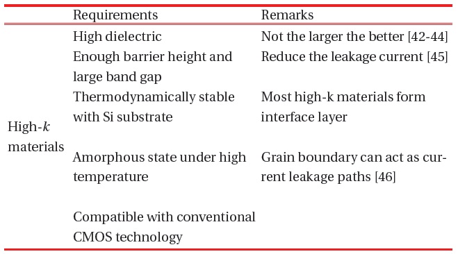
[Table 1.] Some requirements for high-k materials.

Some requirements for high-k materials.
[Table 2.] Performance comparison of some high-k materials [47].
Performance comparison of some high-k materials [47].
2. MECHANISM OF CHARGE STORAGE
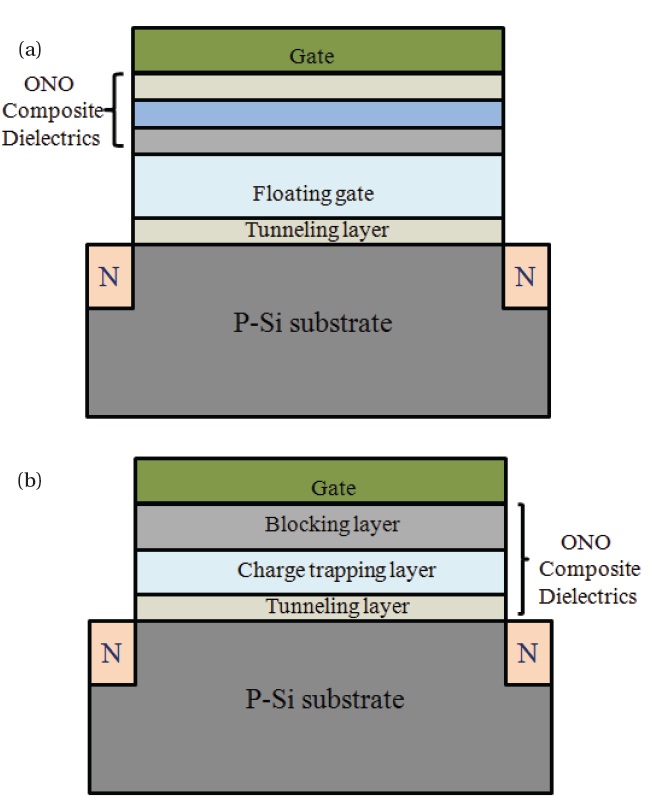
Figure 1 shows the schematic diagrams of the floating gate memory and the SONOS type memory, respectively. In the conventional floating gate-type flash nonvolatile memory, a single defect can discharge the stored charge of the device due to the conductive properties of the floating polysilicon gate electrode.For the case of the SONOS type memory device, however, the charges are stored in discrete traps, since a single defect will not cause the discharge of the whole memory. During the program operation, when a positive gate voltage is applied to the gate electrode relative to the p-Si substrate, the inversion layer form. Electrons tunnel through the tunneling layer into the charge trapping layer and result in a positive threshold voltage shift under the effect of electric field. On the contrary, during the erase operation, holes are injected from p-Si substrate into the charge trapping layer where they are trapped in a manner similar to electrons and lead to a negative threshold voltage shift.
In the past several decades, many efforts have been made to find new materials, structures and technologies in order to meet the requirements, such as low voltage (<5 V), low power programming with long-term retention (>10 years at 85°C) and endurance(>106 write/erase cycles) performance [24]. Employing the high dielectric constant (high-k) materials to replace the sili-con dioxide or silicon nitride in the traditional SONOS/MONOStype devices is a predominant approach.
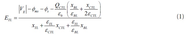
In the semiconductor industry, the requirements for high density and low cost have driven the continuous scaling in the dimensions of metal-oxide-semiconductor field effect transistors(MOSFETs) [25]. However, as the thickness of SiO2 gate dielectrics approaches to 2-3 nm, high leakage current becomes as serious obstacles to future device reliability [26]. In order to overcome these problems, higher permittivity (k) materials,which allows an equivalent capacitance to be achieved using a physically thicker insulating layer, can replace the conventional SiO2 gate dielectric to realize further scaling down. Therefore,in the past several years, much attention have been given to alternative high-k dielectric oxides such as silicates (e.g., Zr and Hf silicate [27, 28]), single metal oxides (e.g., HfO2 [29],ZrO2 [30], Al2O3 [31], La2O3 [32], Pr2O3 [33], Y2O3 [34], Gd2O3 [35],Nd2O3 [36]), and binary metal oxides [37-40]. In order to meet the requirements of CMOS field effect transistors, the high-k dielectrics should satisfy some requirements, as summarized in the Table 1[41].
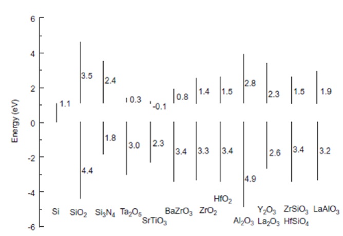
The performance comparison and the predicted band offsets of some high-k dielectrics are given in Table 2 and Fig. 2, respectively. In the conventional SONOS devices, the poor date retention time and the slow program/erase peed are the bottlenecks to limit their applications. The program/erase speed can be enhanced by scaling the tunneling layer thickness. However,the date retention capability becomes worse simultaneously due to the reduction of tunneling layer thickness [48]. To solve this issue, the high-k dielectrics have been investigated widely to obtain a trade-off between the operating speed and the date retention time for SONOS devices.
As an important charge trapping nonvolatile semiconductor memory, SONOS-type devices employ a charge trapping layer to replace the conventional floating gate. However, the conventional Si3N4 charge trapping layer has lower trap density, it cannot meet the requirements of scaling down the charge trapping memories in the future. In addition, traps are considered to originate from defects present in the charge trapping layer,which capture electrons or holes. However, only a certain traps can store charges and maintain a stable memory characteristic after programming, which are considered as effective traps for memory application [49]. To increase the trap densities and to store more charges, adopting high-k dielectrics in the SONOStype memory devices becomes as the predominant approach in the past decades. Up to now, the dominant approach can be subdivided into the following fields: (a) high-k dielectrics as charge trapping layer, (b) high-k dielectrics as charge trapping layer and blocking layer, (c) high-k dielectrics application to three layers,and (d) multilayered structures.
4.1 High-k dielectrics served as the charge trapping layer
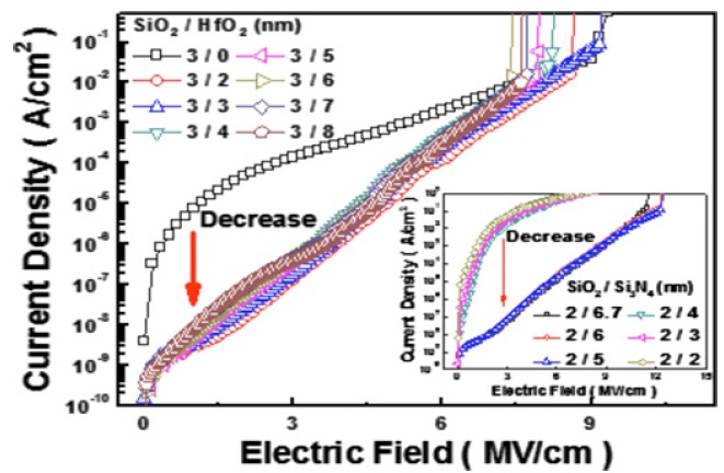
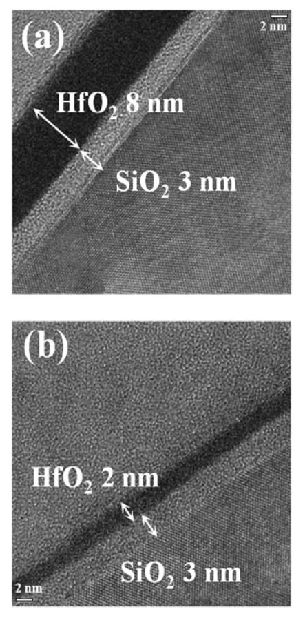
Silicon nitride as the charge trapping layer in the SONOS devices have been studied extensively and the results showed that the devices have poor date retention and scaling issue [50].The high-k materials such as Al2O3, La2O3, ZrO2, and HfO2 in a metal-oxide-high-k-oxide-silicon structure are reported [51-54].HfO2, as the most promising candidate for SONOS devices, has attracted much attention because of its good thermodynamical stability with Si, high dielectric constant, and relatively large band gap (~5.68 eV) [55]. Zhu et al. [56, 57] reported on the electrical properties of HfO2 as the gate dielectric deposited by pulse laser deposition. You et al. [58] deposited HfO2 films with various thickness by atomic layered chemical vapor deposition to replace Si3N4 as the charge trapping layer and formed metal-hafnium-oxide-semiconductor (MHOS) structure. Figure 3 shows the leakage current characteristics MHOS memory capacitors with various thicknesses of HfO2 layer. The data demonstrated that employing stack HfO2 charge trapping layer could decrease the leakage current as compared with a single SiO2 layer. However, the leakage current for the applied electric field is almost the same irrelevant to the thickness of HfO2 charge trapping layer.Inset in Fig. 3 shows the leakage current characteristics of MNOS capacitors with various thicknesses of Si3N4 layer, which indicated that the leakage current of device was reduced by utilizing the HfO2 films as the charge trapping layer and it could obtain larger memory window than the Si3N4 at same trapping layer thickness.The transmission electron microscopy (TEM) images of HfO2/SiO2 stacked layers as charge trapping layer/tunneling layer of MHOS structure capacitors, is shown in Fig. 4. From which, an abrupt interface between the HfO2 layer and SiO2 layer was clearly observed.
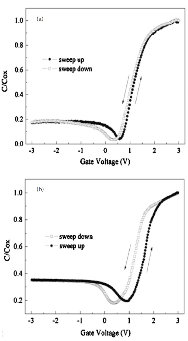
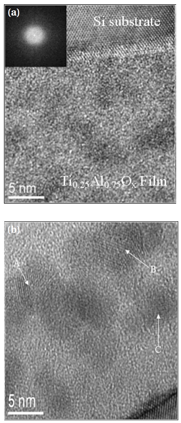
Pan and Yeh [59, 60] also reported a novel high-k SONOS structure using Y2O3 as charge trapping layer. This structure had long charge retention characteristic due to deep trap level and excellent endurance. The group also demonstrated the MONOStype memory device using the high-k NdTiO3 as the charge trapping layer. They deposited ~6 nm Nd2O3 film and ~6 nm Ti film on SiO2 in turn by reactive radio frequency (RF) sputtering. The NdTiO3 film was formed by rapid thermal annealing (RTA) in O2 ambient at various temperatures for 30 seconds. The NdTiO3 MOHOS-type memories have small charge loss rate due to the deep trap levels in high-k layer [48]. Shi et al. [61] found that the pseudo-binary Ti0.25Al0.75Ox film as the gate dielectric exhibited a characteristic of electrical hysteresis after high-temperature treatment. Figure 5 showed the C-V electrical hysteresis curves for pseudo-binary Ti0.25Al0.75Ox films. As shown in Fig. 5, the width of the hysteresis window derived from the Ti0.25Al0.75Ox film annealed at 900°C was much larger than that annealed at 800°C.The phenomenon could be mainly ascribed to the oxygen vacancies created easily at low oxygen partial pressure. Furthermore,the ionization of oxygen vacancies will create conducting electrons and these electrons can be combined with Ti4+ ions to reduce them to Ti3+ ions and/or trapped in oxygen vacancies in turn and lead a positive VFB shift. Therefore, the high-k Ti0.25Al0.75Ox films have promising applications as charge trapping layers. The cross-sectional high-resolution TEM (HRTEM) images of the films annealed at 800°C and 900°C were shown in Fig.6. Clearly, the Ti0.25Al0.75Ox films still remained amorphous state after 800°C annealing, whereas in the films annealed 900°C several crystal regions were obviously observed. The traps in these crystal regions could capture the charges.
4.2 High-k dielectrics served as the charge trapping layer and blocking layer
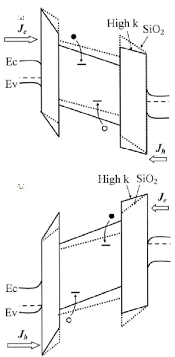
Accordingly, the considerable charge loss through the ultrathin tunneling layer for SONOS/MONOS devices is the formidable obstacle. Lee et al. [62] reported on a new SiO2/SiN/Al2O3 structure that can obtain fast operating speed by Fowler-Nordheim tunneling mechanism. This structure allowed a thicker tunneling layer over 3 nm. The schematic energy band diagram for this structure is shown in Fig. 7. The following equations are used to explain the benefit of this structure under erase mode.
Where ETL and EBL are the electric fields across tunneling layer and blocking layer, respectively. Vg is the erase gate voltage, Φms is the work function difference between the gate and the silicon substrate, Φs is the surface potential, QCTL is the total amount of the charge trapped in the charge trapping layer, xCTL, xTL and xBL are the dielectric constants in the charge trapping layer,the tunneling layer and blocking layer, and xCTL, xTL and xBL are the thickness of the charge trapping layer, tunneling layer and blocking layer, ε0 is the permittivity of free space. By using blocking materials with higher dielectric constant than the tunneling layer, the value of ETL was enhanced, and the EBL was suppressed simultaneously. The results lead to a high operating speed even at a thicker tunneling layer and small gate injection current.
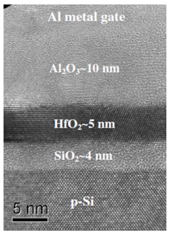
Maikap et al. [63] measured the charge trapping characteristics of p-Si/SiO2/HfO2/Al2O3/metal memory structures. A large memory window of 7.4 V and a high charge trapping density of 1.1 × 1013 cm-2 were reported on the high-k HfO2 charge trapping memory capacitors. These capacitors were treated by RTA at 1,000℃ for 10s in N2 ambient. A typical HRTEM image of a high-k HfO2 charge trapping layer with high-k Al2O3 as a blocking oxide for the memory capacitor, is shown in Fig. 8, in which the HfO2 film is polycrystalline, whereas the Al2O3 film as a blocking oxide is almost amorphous.
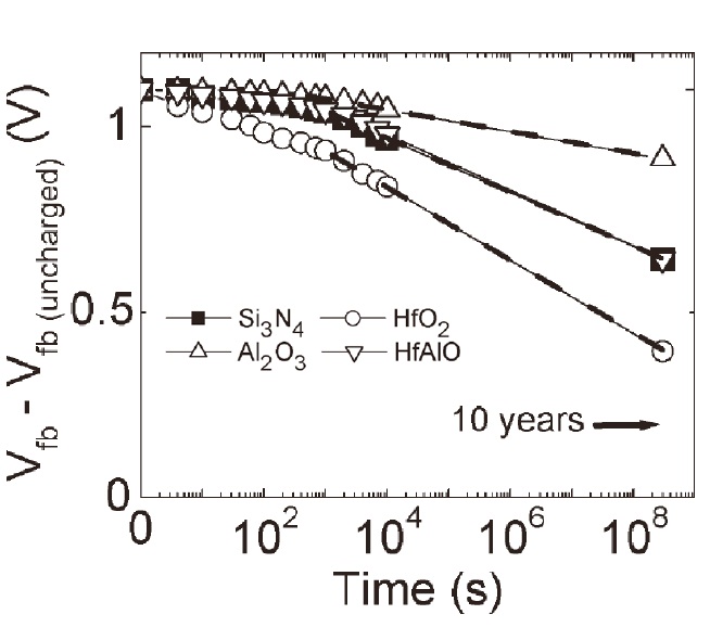
In recently years the (HfO2)x(Al2O3)1-x films as the promising materials are investigated widely [64-68]. Tan et al. [69] used the HfAlO, Al2O3 and Si3N4 films as the charge trapping layers to comparatively investigate the retention performance of memory devices. In addition, they used HfAlO films with different compositional ratios of HfO2 to Al2O3 as a blocking layer, and tested the memory characteristics. The retention characteristics of memory devices with different charge trapping layers were showed in Fig. 9. Clearly, the memory devices with HfO2 as the charge trapping layer exhibited the worst date retention characteristics.The HfAlO-based memory devices have a similar date retention performance to that based on Si3N4, but they are slightly worse than Al2O3. The use of HfAlO films with different compositional ratios of HfO2 to Al2O3 instead of the conventional SiO2 as the blocking layer, results in an increase of the program and erase speeds, especially at low gate voltages. Pu et al. [70] also studied the charge trapping flash memory with (Gd2O3)x (Al2O3)1-x films as blocking layers. Their experimental results demonstrated that the doping of Al into pure Gd2O3 film was an effective way to improve the charge retention of SONOS-type nonvolatile memory, and that 35 mol% Al was the optimized Al concentration in (Gd2O3)x(Al2O3)1-x films. Park et al. [71] further examined the memory characteristics with three different films (Al2O3,Gd2O3 and (Gd2O3)x(Al2O3)1-x) as the blocking layers. Their results demonstrated that addition of Gd into Al2O3 reduced the leakage current, and improved the erase window. The crystallization of the (Gd2O3)x(Al2O3)1-x films leads to a change in the band gap of the (Gd2O3)x(Al2O3)1-x filmd, resulting in a change of the retention properties.
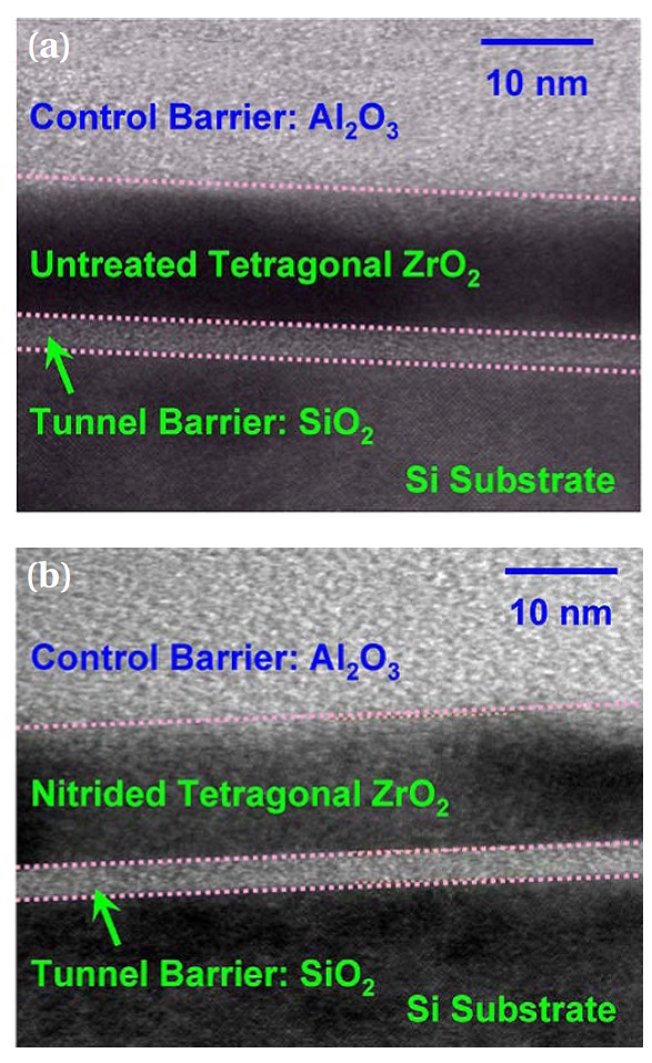
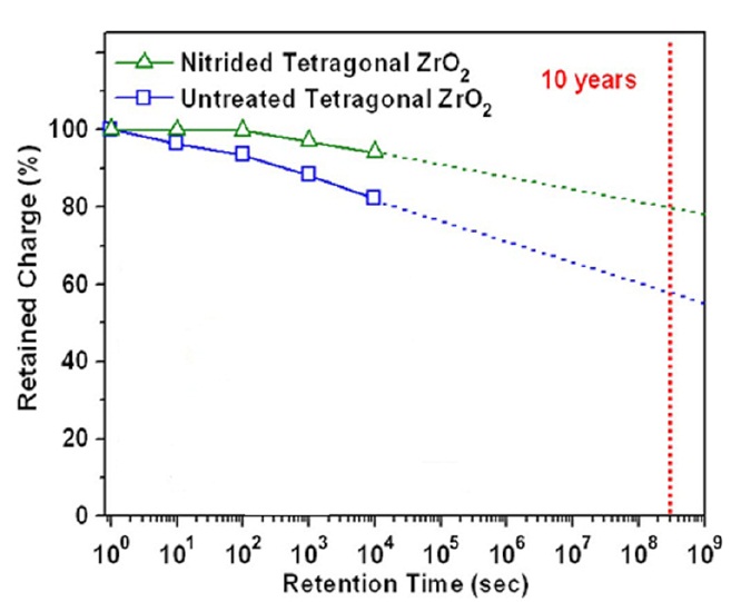
Wu et al. [72] also investigated the memory characteristics of metal/insulator/metal (MIM) capacitors with NH3 nitrided tetragonal ZrO2 film as the charge trapping layer and Al2O3 blocking layer. Figure 10 shows the cross-sectional TEM images of the memory structures with nitrided tetragonal ZrO2 film and untreated tetragonal ZrO2 film as the charge trapping layer. After nitridation, the physical thickness was found to be still kept intact. The data retention characteristics (at 125℃) of the memories with and without NH3 nitridation of the tetragonal ZrO2 film, is shown in Fig. 11. As shown in Fig. 11, the nitride tetragonal ZrO2 films have better data retention and hold the great potential for future high-performance nonvolatile memory, as compared with the tetragonal ZrO2 films without nitridation.
[Table 3.] Performance comparison of MATHS and MHTHS structure[74].
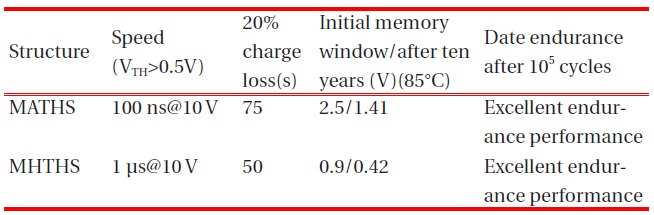
Performance comparison of MATHS and MHTHS structure[74].
4.3 High-k dielectrics served as the tunneling layer,the charge trapping layer and blocking layer
In the future, scaling tunneling layer and ten-year retention requirement at the same time are the key issues to the SONOStype nonvolatile semiconductor memories. Therefore, looking for new high-k materials to replace the tunneling layer is an important subject. Wang et al. [73] fabricated a novel metal/HfO2/Ta2O5/HfO2/Si (MHTHS) structure, which had a 1 μs programming speed and 1 ns erasing speed. Wang and Kwong [74] also employed the TaN/Al2O3/Ta2O5/HfO2/Si (MATHS) structure to obtain fast speed and long retention characteristic. Their experimental results demonstrated that the memory window and programming speed were improved by using Al2O3 to replace HfO2 as the blocking layer. Table 3 presents the performance comparison between the MATHS and MHTHS structures.
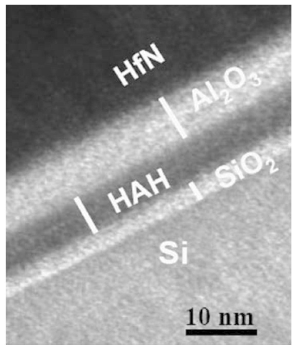
The multilayer tunneling layer concept seems to be a promising route to achieve a trade-off between the operating speed and the date retention due to the redistribution of electric field across the multilayer tunneling layer compared with a single tunneling layer, making the tunneling layer thinner at the same applied bias [75-84]. Chen et al. [85] fabricated a memory capacitor with a multistacked tunneling layer of Al2O3/HfO2/SiO2 (AHO) together with HfO2 charge trapping layer and Al2O3 blocking layer. As compared to a single SiO2 tunneling layer, the multistacked tunneling layer, can offer a large memory window(7.6 V) for ±12 V sweep voltage range and an improved date retention characteristic. Ding et al. [86] also reported on a novel multilayered structure of SiO2/HfO2-Al2O3-HfO2 (HAH)/Al2O3/HfN as the charge trapping layer, where HAH multilayer possess of better thermal stability and higher charge storage capability compared to pure HfO2 film [87]. A cross-sectional TEM image of the SiO2/HAH/Al2O3/HfN memory capacitor, is shown in Fig.12, and sharp interfaces within the Si/SiO2/HAH/Al2O3/metal structure are clearly observed. This memory capacitor exhibits a sufficient electron and hole trapping efficiencies such as an electron density of ~7 × 1012 cm-2 under 13 V program for 0.5 ms and a hole density of ~4 × 1012 cm-2 under -12 V erase for 0.5 The multilayer tunneling layer concept seems to be a promising route to achieve a trade-off between the operating speed and the date retention due to the redistribution of electric field across the multilayer tunneling layer compared with a single tunneling layer, making the tunneling layer thinner at the same applied bias [75-84]. Chen et al. [85] fabricated a memory capacitor with a multistacked tunneling layer of Al2O3/HfO2/SiO2 (AHO) together with HfO2 charge trapping layer and Al2O3 blocking layer. As compared to a single SiO2 tunneling layer, the multistacked tunneling layer, can offer a large memory window(7.6 V) for ±12 V sweep voltage range and an improved date retention characteristic. Ding et al. [86] also reported on a novel multilayered structure of SiO2/HfO2-Al2O3-HfO2 (HAH)/Al2O3/HfN as the charge trapping layer, where HAH multilayer possess of better thermal stability and higher charge storage capability compared to pure HfO2 film [87]. A cross-sectional TEM image of the SiO2/HAH/Al2O3/HfN memory capacitor, is shown in Fig.12, and sharp interfaces within the Si/SiO2/HAH/Al2O3/metal structure are clearly observed. This memory capacitor exhibits a sufficient electron and hole trapping efficiencies such as an electron density of ~7 × 1012 cm-2 under 13 V program for 0.5 ms and a hole density of ~4 × 1012 cm-2 under -12 V erase for 0.5
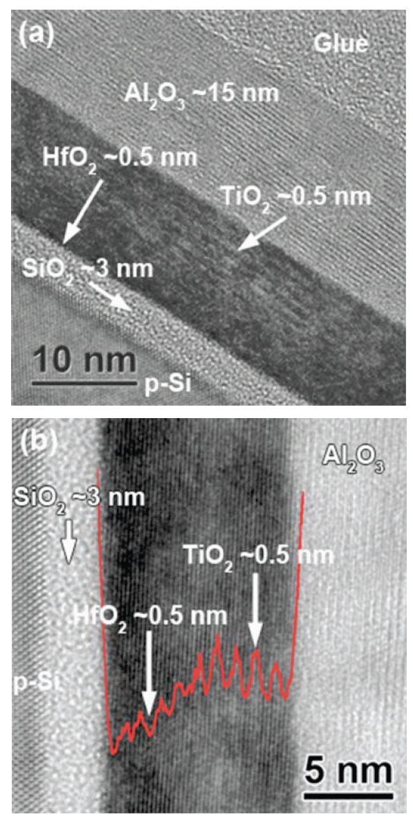
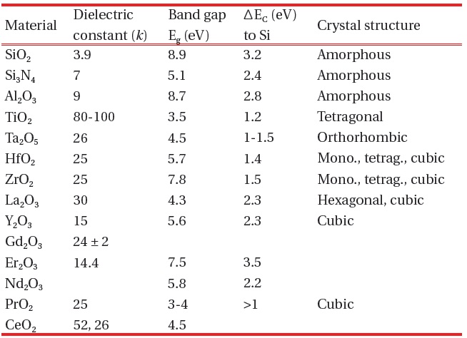
The high-k HfO2/TiO2 multilayers in p-Si/SiO2/(HfO2/TiO2)/Al2O3/aluminum memory capacitors exhibit a memory window of ~5 V at gate voltage of ±5 V due to exiting much quantum wells in the multilayered structure.
5. CONCLUSIONS AND PERSPECTIVE
For conventional floating gate-type nonvolatile semiconductor memories, the challenge is to achieve reliable, low-power,low-voltage performance with the further scaling of device size.Therefore, new flash NVSM technology will be required to overcome these issues. As the promising candidates to replace the conventional floating gate nonvolatile semiconductors memory,SONOS-type memory devices have been investigated widely in the past several years. However, the operating speed and date retention characteristics are bottlenecks for SONOS-type memory devices. Employing high-k dielectrics as the charge trapping layer, tunneling layer and blocking layer in these devices is a predominant approach to realize a trade-off between the operating speed and the date retention time. It is found that the single metal oxide (e.g., HfO2 and ZrO2) are promising alternative to replace the conventional Si3N4. Using rare earth metal oxide as charge trapping layer, such as Y2O3, also can improve the memory characteristics. Doping Al2O3 into HfO2 forming binary oxide can obtain a trade-off between operating speed and date retention time. Lee et al. [62] proposed a novel SiO2/SiN/Al2O3 structure, in which the conventional blocking layer of SiO2 was replaced by Al2O3. By using blocking materials with higher dielectric constant than the tunneling layer, the electric fields across tunneling layer (ETL) was enhanced and the electric fields across blocking layer (EBL) was suppressed simultaneously. This memory structure has fast operating speed via Fowler-Nordheim tunneling mechanism and allows for a thicker tunneling layer over 3 nm. At present, most researches are focused on SONOS-type memories based on this type structure. Multilayered structures, including multilayered tunneling layers or charge trapping layers, are also a promising approach to improve the memory characteristics.
As the development of nonvolatile semiconductor memory technology, the high-k dielectrics will replace the conventional Si3N4 as the charge trapping layer to obtain higher trap density and small leakage current. Al2O3 is typical blocking material in SONOS structure because of high barrier height and feasible permittivity (~9). In the short term, Al2O3 as the blocking layer can satisfy the requirements. However, in the long run,employing high-k blocking dielectrics, which have larger permittivity than Al2O3, will be required for further scaling of the thickness. When the thickness of SiO2 approaches to 2 nm, the leakage current become formidable. Since, in order to realize trade-off between date retention time and operating speed,using high-k dielectrics or stacked structures as the tunneling is necessary.

![Performance comparison of some high-k materials [47].](http://oak.go.kr/repository/journal/12908/E1TEAO_2010_v11n4_155_t002.jpg)
![Predicted band offsets for various high-k oxides [47].](http://oak.go.kr/repository/journal/12908/E1TEAO_2010_v11n4_155_f002.jpg)
![Leakage current characteristics of metal-hafnium-oxidesemiconductorcapacitors with various thicknesses of HfO2 layer.Inset shows tunneling current characteristics of metal-nitride-oxidesiliconcapacitors with various thicknesses of Si3N4 layer [58].](http://oak.go.kr/repository/journal/12908/E1TEAO_2010_v11n4_155_f003.jpg)
![Transmission electron microscopy images of HfO2/SiO2 layerson Si substrates. (a) HfO2 = 8 nm and (b) HfO2 = 2 nm [58].](http://oak.go.kr/repository/journal/12908/E1TEAO_2010_v11n4_155_f004.jpg)
![C-V measurements of the Ti0.25Al0.75Ox capacitors measured at 1MHz and annealed at (a) 800℃ and (b) 900℃, respectively [61].](http://oak.go.kr/repository/journal/12908/E1TEAO_2010_v11n4_155_f005.jpg)
![Cross-sectional high-resolution transmission electron microscopyimages of the Ti0.25Al0.75Ox films annealed at (a) 800℃ and (b)900℃ [61].](http://oak.go.kr/repository/journal/12908/E1TEAO_2010_v11n4_155_f006.jpg)
![Comparison of schematic energy band diagram for the conventionalSONOS (dashed line) structure and the SHNOS (solid line)structure at the write mode (a) and erase mode (b) [62].](http://oak.go.kr/repository/journal/12908/E1TEAO_2010_v11n4_155_f007.jpg)
![High-resolution transmission electron microscopy image ofa high-k HfO2 charge trapping layer with high-k Al2O3 as a blockingoxide for a memory capacitor [63].](http://oak.go.kr/repository/journal/12908/E1TEAO_2010_v11n4_155_f008.jpg)
![Flat band voltage versus time of SONOS-type memory deviceswith Si3N4, Al2O3, HfO2, or HfAlO as the charge trapping layers [69].](http://oak.go.kr/repository/journal/12908/E1TEAO_2010_v11n4_155_f009.jpg)
![Cross-sectional transmission electron microscopy images forthe memory structures with (a) untreated and (b) nitrided tetragonalZrO2 films [72].](http://oak.go.kr/repository/journal/12908/E1TEAO_2010_v11n4_155_f010.jpg)
![Comparison of the retention characteristics at 125℃ for thememory devices with and without nitridation of the tetragonal ZrO2films [72].](http://oak.go.kr/repository/journal/12908/E1TEAO_2010_v11n4_155_f011.jpg)
![Cross-sectional transmission electron microscopy image ofthe SiO2/HfO2-Al2O3-HfO2 (HAH)/Al2O3/HfN memory capacitor [86].](http://oak.go.kr/repository/journal/12908/E1TEAO_2010_v11n4_155_f012.jpg)
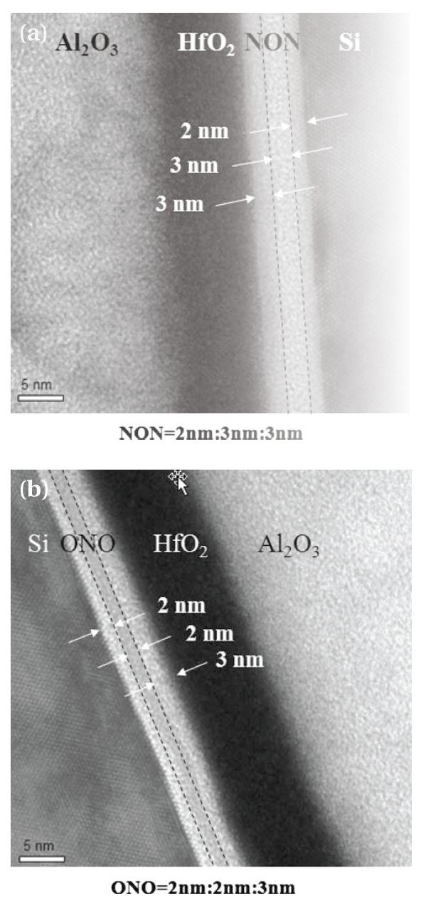
![Transmission electron microscopy images of SiO2/Si3N4/SiO2(ONO) and Si3N4/SiO2/Si3N4 (NON) tunneling layers with HfO2 ascharge trapping layer and Al2O3 as blocking layer [88].](http://oak.go.kr/repository/journal/12908/E1TEAO_2010_v11n4_155_f013.jpg)
![(a) High-resolution transmission electron microscopy (HRTEM)image of high-k HfO2 (0.5 nm)/TiO2 (0.5 nm) multilayers withten periods in p-Si/SiO2/(HfO2/TiO2)/Al2O3 structure after annealingat 900℃ for 1 minute in N2 ambient. (b) HRTEM image with elementalline profile by DIGITAL MICROGRAPH software shows the clearHfO2/TiO2 layer-by-layer structure (red color) [89].](http://oak.go.kr/repository/journal/12908/E1TEAO_2010_v11n4_155_f014.jpg)
![Performance comparison of MATHS and MHTHS structure[74].](http://oak.go.kr/repository/journal/12908/E1TEAO_2010_v11n4_155_t003.jpg)