Tin oxide (SnO2) has been extensively studied as a transparent conducting oxide for optoelectronics, photovoltaics, catalysts, and gas sensors. SnO2 films have been fabricated using various technologies, including sputtering [1], chemical vapor deposition [2], spray pyrolysis [3], and atomic layer deposition (ALD) [4,5]. Among these, ALD demonstrates unique film properties as compared to the other fabrication technologies, which result in obtaining a dense and high aspect ratio of film with fewer defects. ALD is an ideal technology for depositing ultrathin film with high conformality and precise thickness control by using alternating self-controlled chemical process between gases precursor and a solid surface to deposition materials in an atomic layer-by-layer fashion. Plasma enhanced ALD (PEALD) is a promising technology for obtaining high quality metal oxide films at relatively low temperatures, as compared with commercial chemical vapor deposition (CVD). Interestingly, a comparative study of the growth of tin oxide films by ALD and CVD, using the SnI5 and O2 precursor combination, has been reported [6]; in both cases the films were tetragonal rutile-type. The thin films grown by ALD, found to be very close to single crystalline, contained a low amount of defects and were nearly atomically smooth. The CVD films had much rougher film morphology an exhibited both grain boundaries and twin formation.
Tin oxide thin films have been previously fabricated by ALD using halogenated precursors, SnCl4 and SnI4, and non-halogenated precursors, tetrakis (dimethylamino) tin and dibutyltin diacetate [4,5,7]. By using a halogenated precursor, high deposition temperature and low growth rate with corrosive problems were reported. Among non-halogenated pre-cursors, dibutyltin diacetate showed tin films with an eight sec purging time at 50 to 300℃ [5]. From a non-halogenated precursor of tetrakis(dimethylamino) tin oxide film was deposited at an average growth rate of 1.2 A/cycle at 50 to 300℃ by using a seeding method of ALD; a seed material was used, comprised of 1 nm Al2O3 with trimethyl aluminum, by ALD [4].
We prepared tin oxide films by plasma-enhanced ALD using tetrakis (ethylmethylamino) tin as a non-halogenated precursor with various temperature ranges [8]. As a seed material, zinc oxide was used to examine the seeded growth effect of tin oxide. Growth rate, structural, morphological, and compositional analyses, were performed with as-deposited and thermally annealed thin films.
The ALD experiments used a bubbler type source delivery system with separately installed gas purge lines. Tin oxide was grown as an insulating layer on a 4" p-type silcone (100) wafer after plasma cleansing. The tin oxide precursor was tetrakis (ethylmethylamino) tin. Oxygen plasma was used as the oxygen source. The reaction temperature of the process module was controlled in the range of 50 to 200℃. The reactor pressure was maintained at 0.8 Torr with an Ar purging of 100 sccm. During the reaction process, the tin precursor and oxygen plasma were sequentially injected into the reactor chamber to form a tin oxide monolayer on the substrate. An ALD cycle consisted of the injection of diethyl zinc for 0.005 seconds, Ar pursing for 2.0 seconds, O2 gas for 2.0 seconds, and radio frequency power of 100 W. Then tin precursor for 4.0 seconds, Ar purging, O2 gas for 2 seconds, and 2 additional seconds with radio frequency power of 100 W, and final gas purging. The crystalline phase of the tin oxide film was characterized by XRD using Cu-Ka radiation operated at 35 KV. The microstructure was examined by a field emission scanning microscope (FE-SEM, Joel). The surface morphology was examined by AFM (PSIA, XE-150). An ellipsometer (Gartner L116D) was used for thickness analysis. The XPS analysis was performed by a Thermo VG ESCA Sigma Probe spectrometer using a monochromatric Al-Ka radiation source from an X-ray operated at 15 kV and 100 W. The surfaces of the specimens were cleaned by Ar+ etching (2 kV, 1.8 μA) prior to recording a spectrum. The spectra were calibrated by C1 s (285 eV).
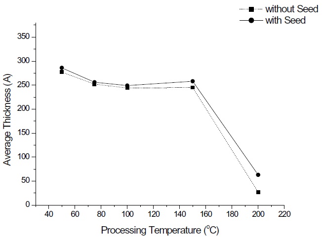
Figure 1 shows the average growth rate of tin oxide thin films with substrate temperatures. At low temperatures the average growth rate is over 1.2 A/cycle; this is higher than that the growth rate of 0.7 A/cycle when using SnCl2. However, the growth rate dramatically decreases to negligible film formation at 200℃. In the case of the seeded reaction of zinc oxide, the average growth rate slightly increased to 1.45 A/cycle. Generally, the growth rate of tin oxide by vacuum deposition methods, such as ALD, CVD, and sputter, is relatively high at low temperatures and decreases as the temperature increases. Previous results of other precur-sors with a hydroxyl peroxide reactant reported that the average growth rate of tin oxide by ALD exhibited 1.2 A/cycle between 100 and 200℃ with a subsequent rate drop above 250℃ due to the precursor's decomposition at the higher temperature [4]. Our results were very similar with the exception of the growth rate rapidly dropping at 200℃, as opposed to 250℃. The reason for this may be incomplete absorption of the precursor on the sub-strate at the higher temperature; nucleation of tin oxide at the higher temperature may not be possible. Other researchers have used a seed material of 1 nm Al 2 O 3 with trimethyl aluminum by ALD to promote the prompt nucleation of SnO2[4]. Without the initial step of the seeding of Al 2O3, thinner SnO2 films showed greater variations in thickness. This thickness variation was not observed in our process. Different results were reported using a dibutyltindiacetate precursor for tin oxide deposition [5]. The thickness increased with substrate temperatures up to 400℃. The precursor properties are critical for the film fabrication by ALD.
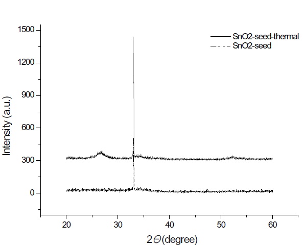
From the XRD characterization in Fig. 2, the crystallinity of the as-deposited film is difficult to determine at 150℃ substrate temperature for both cases of with and without a seed layer. However, (110) peak around 27 degrees appears as dominant after being thermally annealed at 600℃ for 30 min. Interestingly, a trace of (220) peak around 53 degrees, (101) peak around 34 degrees, and (200) peak around 39 degrees are detected after thermal annealing. The (110) crystalline surface of the tin oxide is thermodynamically the most stable and is the predominant crystal face [9]. The as-deposited and seeded tin oxides demon-strate the same behavior by XRD; for both cases, there is no crys-tallinity for the as-deposited films and only a slightly increased crystallinity of the thermally annealed films.
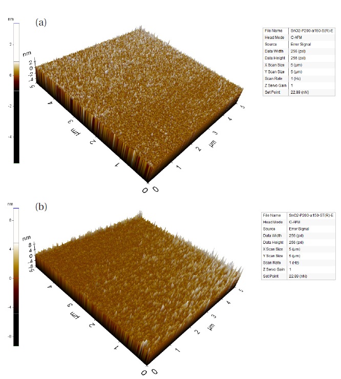
The surface morphology and roughness of the tin oxide samples of 100℃ process sample, as-deposited and thermal annealed, were characterized by AFM. As expected, a dense tin film by ALD was observed. The root mean square roughness (Rq) and average roughness (Ra) of the as-deposited tin films are 0.264 nm and 0.209 nm, tively, while the thermally annealed tin oxide films are 0.588 nm and 0.464 nm, tively. In the case of the zinc seeded deposition of the tin oxides, the Rq and Ra of the as-deposited tin films are 0.348 nm and 0.276 nm, tively, while the thermally annealed are 0.708 nm and 0.630 nm, tively. Interestingly, the roughness is relatively good even though the grains levels are increased after thermal annealing; post-annealing results indicate a more pronounced texture and grain growth. The morphology and roughness variation of the thin films are due to the coalescence or migration of the grains. In this process, the morphology of the needle-like texture was observed to be different from the sierra valley-like texture with the dibutyltin diacetate precursor [5].
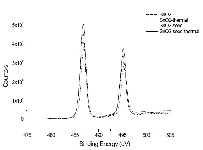
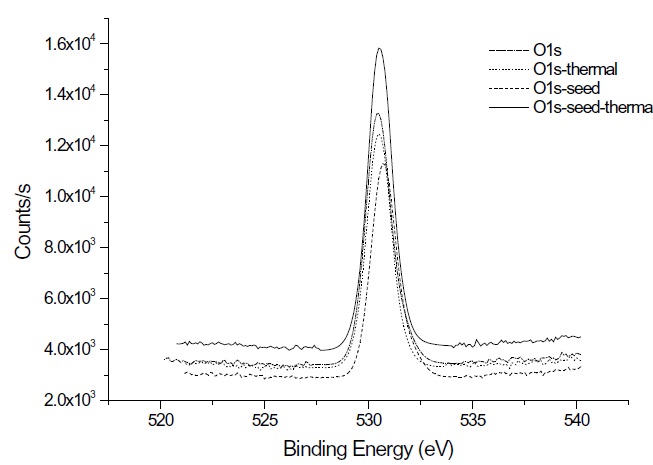
XPS measurements were performed to verify the tin oxide components and composition under the process conditions and thermal treatment. Figure 4 shows the XPS data of the Sn 3d spectra of the 200 cycled as-deposited films at 50℃ and the thermally annealed film at 600℃ for 30 min. The binding energy of the Sn4+ peak and Sn2+ peak are 487.2 eV and 486.2 eV, respectively, similar to other research findings [9]. The binding energy of the Sn 3d5/2 peak can be assigned to 486.7 eV for both tin oxide and thermally treated tin oxide. In the case of the seeded tin oxide deposition, the peak is assigned to 487.0 eV and 486.8 eV, before and after thermal annealing, respectively. The XPS mea-surement of oxygen in a tin oxide film is shown in Fig. 5. Various types of oxygen status demonstrate various binding energies, such as: 530.7 eV for O-, 530.1 for O2-, and 530.6 eV and 532.8 eV for O2-. These oxygen statuses are also affected by process parameters. From Fig. 5, the single peak of 530.5 eV might be assigned to O-.
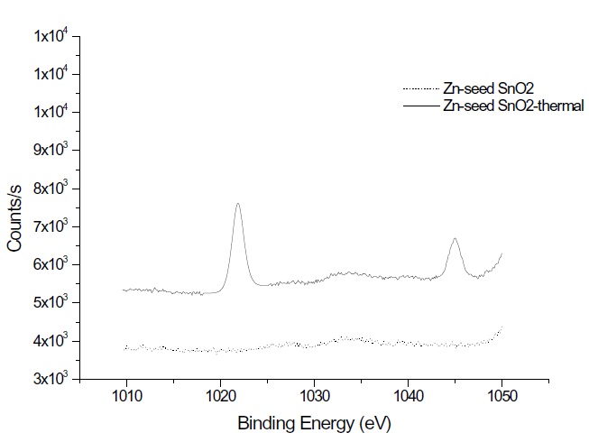
Tin oxide can assume a different stoichiometric, such as SnO, Sn3O4, and SnO2. ALD performed at 325℃ using SnCl 4 /H2O2 produced SnOx , while SnCl4/H2O at 500℃ produced SnO2 film [10]The atomic ratios of [Sn] : [O] in the XPS spectrum are estimated to be 45.72 : 54.28 and 45.70 : 54.30 for as-deposited without and with seed, tively, and 46.80 : 53.20 and 44.28 : 54.12 for thermally annealed without and with seed, tively. The XPS measurement in this study yields SnO x with x = 1.14 to 1.27, suggesting that the thin films are mostly SnO. That may be related to the XPS's nanometer probing depth, which reflects an oxygen deficient SnO surface layer. Thermal annealing slightly increases the amount of tin in a thin film. The precursor chemistry is im-portant; with a halogenated precursor, the chloride based tin oxide ALD process has a slower growth rate than that the corresponding iodide based process [11]. Interestingly, the Zn seed layer effect has minimal influence on the compositions during the ALD process. However, the Zn amount increases to 1.6% of the total composition of the thin film after thermal annealing. Zn crystal growth is confirmed by XPS of the seeded SnO2 with thermal annealing, as shown in Fig. 6. The growth rate of Zn crystals increases with an increase in the substrate temperature.
In order to prepare tin oxide thin films by ALD, with and without a seed layer, a precursor tetrakis-(ethylmethylamino) tin was prepared. The average growth rate of tin oxide film is approximately 1.2 to 1.4 A/cycle from 50 to 150℃; this increases slightly with a seed layer. The growth rate rapidly decreases at the substrate temperature of 200℃. The amorphous thin film was prepared using ALD and the crystallinity was increased with thermal annealing. AFM revealed the morphology of the film was a needle-like texture. The roughness of the deposited tin film shows good. The atomic ratios of [Sn] : [O] in the XPS spectrum are estimated to be 1: 1.19. The thermal annealing effects are a slight increase in surface roughness and an higher amount of tin in the composition, with associated crystallinity.