Energetic materials are a class of materials having high amounts of stored chemical energy that is able to be rapidly released in the form of thermal energy. Energetic materials are generally composed of an oxidizer and a fuel which are physically mixed together. Energetic materials are used in explosives,pyrotechnics, and propellants; their properties make it possible to produce a greater amount of energy as compared to the input energy. Many technologies used for synthesizing nanoenergetic materials have been proposed. One of the simplest methods is a nanopowder mixed with fuel metal and oxidizer particles [1]. In addition, nanoenergetic materials can also be prepared by solgel[2], nanostructured multilayer foils [3,4], and nanocrystalline porous silicon with oxide [5]; these methods have difficulty in obtaining a homogeneous mixture, as well as hazardous and elaborate procedures. In this study, Al/CuO-based nanoenergetic materials were produced by integrating CuO nanowires grown from Cu thin film with nano-Al deposited onto a glass substrate.The fabricated nanoenergetic materials were characterized by scanning electron microscopy (SEM), X-ray diffraction (XRD),and differential scanning calorimetry (DSC). We investigated the heat flows and heat energies released from the CuO nanowires with deposited nano-Al; the results suggest that these could potentially be used for a-Si crystallization [6].
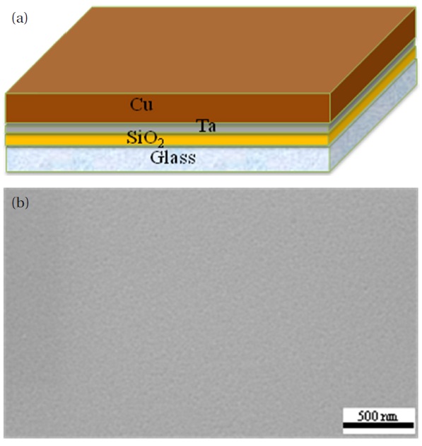
The nanoenergetic material sample was prepared as shown in Fig. 1. Figure 1(a) shows the deposited Cu film as well as the other layers. 1-um-thick Cu thin film was deposited onto a glass substrate by RF sputtering. A 100-nm-thick SiO2 film as a buffer layer and a 50-nm-thick Ta film as an adhesion layer were also deposited onto the glass substrate by RF sputtering. Figure 1(b)shows the top-view SEM image of the deposited Cu layer without the nano-wire structure. The native oxides of the Cu thin films were removed by a solution of 10 ml HCl and 60 ml de-ionized water. The samples were placed in a quartz tube in the middle of a horizontal tube furnace; static air was used for annealing. The samples were annealed in a horizontal tube furnace at various temperatures for four hours, in order to determine the optimum annealing temperature. The annealed samples were allowed to naturally cool to prevent peel-off due to thermal stress. CuO nanowires grew from the 1-μ-thick Cu thin film [7]. Nanoenergetic materials were produced by depositing a 1-μ-thick Al on top by RF sputtering. The CuO/Al-based nanoenergetic materials on the glass substrate were characterized by SEM and XRD. The thermite reaction of CuO nanowires with the deposited nano-Al was investigated using Joule heating. The heat released by the interfacial reactions was measured using DSC with an air flow rate of 20 ml/min and a heating rate of 10℃/min. DSC was carried out from 100 to 700℃. The final reaction compositions were identified by XRD after DSC analysis.
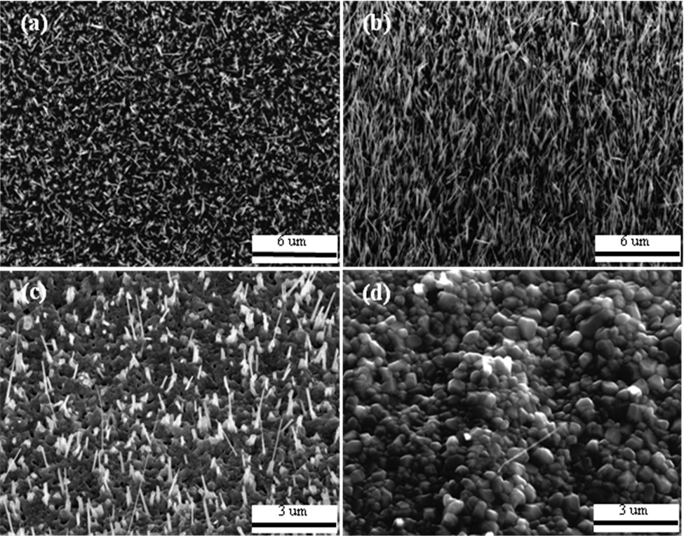
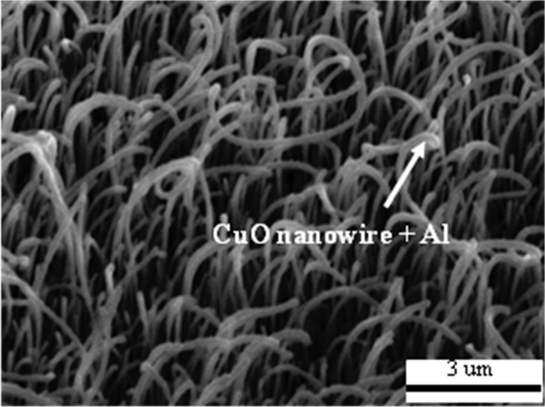
In order to study the influence of annealing temperatures on the growth of CuO nanowires, the samples were annealed in a horizontal tube furnace at various temperatures for four hours. Figure 2 shows the 30°-tilted SEM images of the Cu films annealed in static air for four hours at 400℃, 500℃, 600℃, and 700℃. Uniform CuO nanowires only grew in the temperature range from 400 to 500℃, as shown in Fig. 2(a) and (b). Only a few nanowires were formed when the temperature was 600℃ or higher, as shown in Fig. 2(c). When the temperature was 700℃or higher, no nanowires were formed and the film surface was coated with small particles, as shown in Fig. 2(d). Based on the SEM images of the CuO nanowires, the optimum annealing temperature condition was determined to be 500℃ for four hours,thus yielding uniform CuO nanowires. Figure 3 shows 30°-tilted view SEM images of the CuO nanowires coated with uniformly deposited nano-Al.
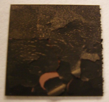
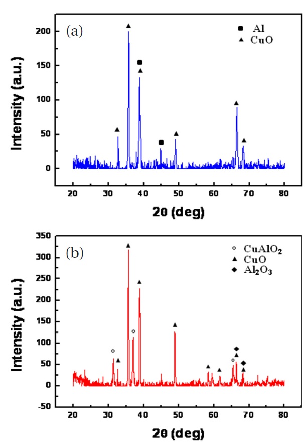
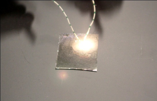
As previously mentioned, high temperature annealing induced thermal stress might cause the film cracks shown in Fig.4. To avoid film cracking, the film was allowed to naturally cool down in the furnace after thermal annealing. Figure 5 shows the XRD patterns of the CuO nanowires with deposited nano-Al. Only CuO and Al diffraction lines can be seen from the XRD patterns as shown in Fig. 5(a). There is no Al2O3 peak, indicating that no major reaction between Al and CuO nanowires occurred during the Al deposition, presumably due to the strong vacuum and low substrate temperature. Figure 5(b) shows the XRD pattern of the nanocomposite after DSC analysis. The final reaction products were identified as CuAlO2, CuO, and Al2O3; CuAlO2 is formed from the reaction of Al2O3 and CuO. The XRD pattern did not show the Cu and Al lines that should be present after reduction of CuO by Al. The photograph in Fig. 6 shows a bright flash of light produced by the explosive reaction between the CuO nanowires and the deposited nano-Al. The thermite reaction was ignited by Joule heating. The adiabatic frame temperature would potentially be above 2,000℃ [8]. The thermite reaction between CuO nanowires and the deposited nano-Al can be written as

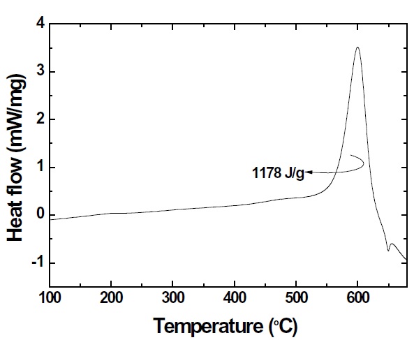
where △H is the energy released during the reaction. To investigate the heat flows and onset temperatures of the exothermic reaction between the CuO nanowires and the deposited nano-Al, the nanoenergetic materials were characterized using DSC with a maximum temperature of 700℃, as shown in Fig. 7. An exothermic reaction peak was produced by the thermite reaction between the CuO composite and the nano-Al. The DSC plots of the heat flow for the exothermic reaction shows the exothermic reaction peak of the CuO nanowires coated with deposited nano-Al. Integrating the area of the first exothermic reaction peak with DSC is the heat energy released by the exothermic reaction. The first exothermic reaction peak represents the nanocomposites prior to the aluminum melting peak at 660℃. Nanoenergetic materials were achieved by the deposition of nano-Al on CuO nanowires, which resulted in good interface contact and reactivity.Impurities and Al oxidation were reduced by deposition in a strong vacuum and at a low substrate temperature. In this study,the heat energy from DSC was measured; it was approximately 1,178 J/g, which was higher than the 1,024 J/g of a previous research study for selective area crystallization of a-Si [9]. CuO nanowires coated with deposited nano-Al can be used as a crystallization energy source of a-Si.
CuO nanowires on which nano-Al had been deposited were synthesized using a horizontal tube furnace and RF sputtering.CuO nanowires were grown from Cu film deposited onto a glass substrate after annealing. The best annealing conditions were found to be four hours at 500℃. The length of the CuO nanowire was greater than 3 μ. To induce a thermite reaction, nano-Al was deposited onto the CuO nanowires. A thermite reaction was induced by Joule heating. The heat energy was higher than the energy for a-Si crystallization. Finally, this thermite reaction could potentially be used for selective area crystallization of amorphous silicon films.