Anodic aluminum oxide (AAO) is a nanoporous structure consisting of a typical self-ordered nanochannel material, which has various nanotechnological applications [1-4]. The material,which is formed by anodizing aluminum (Al) in an appropriate acid solution, is usually composed of many hexagonally arranged cells with cylindrical pores in the center [5]. The porous structure exhibits locally ordered close-packed quasi-hexagonal arrays with alumina walls. This nanoporous structure is very useful as a template to form various one-dimensional (1D) nanoscaled materials, such as photonic crystals, nanowires, and nanofluidic channels [6-11].
The mechanism of the porous AAO was extensively investigated in terms of the pore parameters, such as the pore diameter and the length, which are determined largely by the anodization conditions, such as the applied dc-voltage, pH of the acid, and anodization time [12-14]. The anion, or negative ion, is attracted to the Al anode, the anion joins to the cation at the Al/oxide interface for the chemical reaction of Al-O bonds for AAO formation,and the electric field-assisted dissolution happens through the counter-diffusion of the oxide carrying the Al ions [15,16].The anodization process has a theoretical mechanism of pore formation as a result of the competing oxidation and dissolution processes [17-20]. In order to completely understand the AAO formation mechanism, it is necessary to clarify the effect of the electric field on the geometrical curvature in the nanochannel formation.
In this work, we have investigated the formation mechanism of the nanoporous structure in the anodization process of Al foil. The nano-channel can be strongly correlated with the initial curvature of the Al surface in the oxidation mechanism, and the surface normal is consistent with the electric field direction that evolves during the anodic etching process.
Al foil samples were prepared for the anodization process in order to produce the AAO templates [21]. The mirror-like surface of the Al plate was created by an electro-polishing pretreatment in a mixed solution (HClO4 [60%]: C2H5OH = 1:4). During the electro-polishing process, the ultrasonic cleaning was carried out in acetone liquid for 3 minutes. Electric power was applied to the voltage of 20 V for 60 seconds at 3℃. The sample was dipped in an ethanol solution for 20 minutes, and the solvent was then rinsed out in de-ionized water several times.
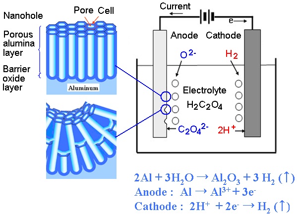
The Al plate was anodized by using a two-step anodization procedure as shown in Fig. 1. The first anodization was performed by applying a DC voltage of 40 V and a current of 0.1 A to a 0.3 M oxalic acid (H2C2O4) solution at 3℃ and 15℃ for 20 minutes to form the pore layer evenly. In order to obtain a wellordered nanoporous alumina layer, the alumina formed during the first anodization process was completely removed with wet chemical etching. Wet chemical etching is done in a mixed solution (0.2 M CrO3, 0.4 M H3PO4) for 1 hour. The second anodization was performed under the same conditions as the first anodization. Finally, the pore widening was performed in a 0.1 M H3PO4 solution at 30℃.
Figure 2 shows the scanning electron microscope (SEM) images of AAO on the Al plate in the second anodization process.After the removal of the first anodized layer of AAO, the Al surface has a nanostructural pattern, which covers the initial curvature in Fig. 2(a). When the diameter of the curvature is large, there are nanopatterns in the inner surface of the curvature. Under a dc bias of 40 V, the second anodization process was performed, and a sunken or crater-like place on the surface formed the nanochannels, which are normal to the initial surface as shown in Figs. 2(b) and (c). The nanochannels formed in the direction of the surface normal compete with those from the flat surface zone. This results in the convex curvature on the barrier layer as shown in Fig. 2(d).
In the anodization process, the conducting electrolyte forms an equipotential plane on the Al surface, so the electric field is aligned in the same direction as the nanochannel in the AAO formation.In a crater-like surface with a large diameter, chemical reactions occur to form the array of nanoholes. The size of the nanohole diameters is related to the dc bias, as does the alumina barrier. This is the same for a flat surface. When the diameter of a crater is small enough to form a single nanohole, the electric field plays a driving force in forming a nanochannel. This phenomenon is similar to the AAO formation with the surface nanoindentation process, where the Al surface is pretextured [22,23]. At a nanoindented site on the flat Al surface, a single nanohole forms a straight nanochannel under the uniform electric field.
However, when a single nanohole located on the curved surface need to modify the direction of the nanochannel due to the perturbation of electric field for metastable minima in equipotential plane. The single nanochannel can be split into two nanochannels,since the space is too big to form a single nanochannel,and to keep a constant dimension for the nanoholes. We can observe the split nanochannels in detail.
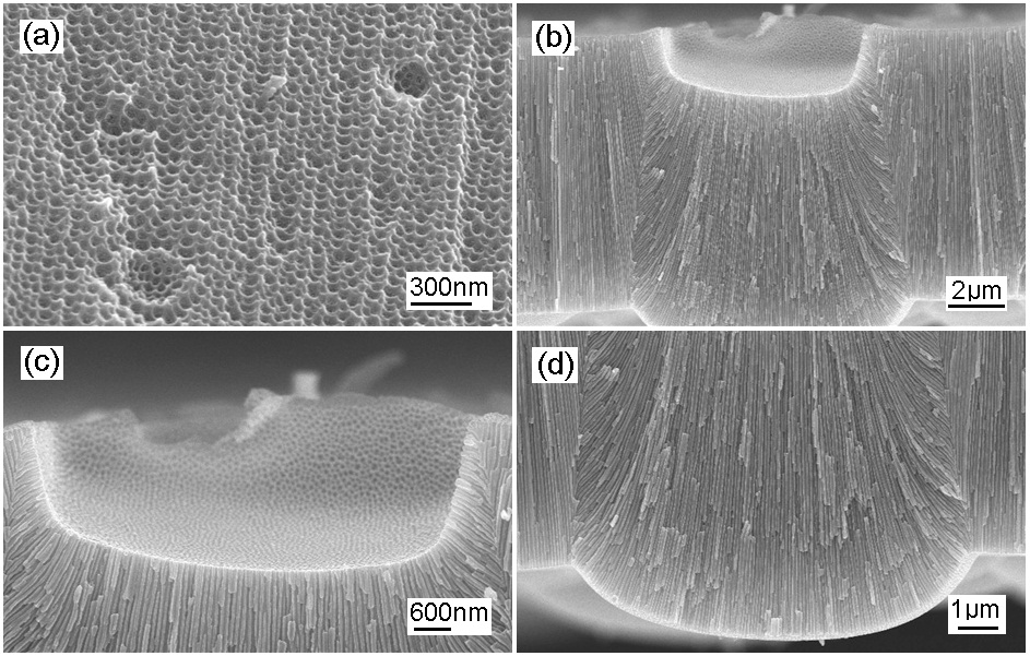
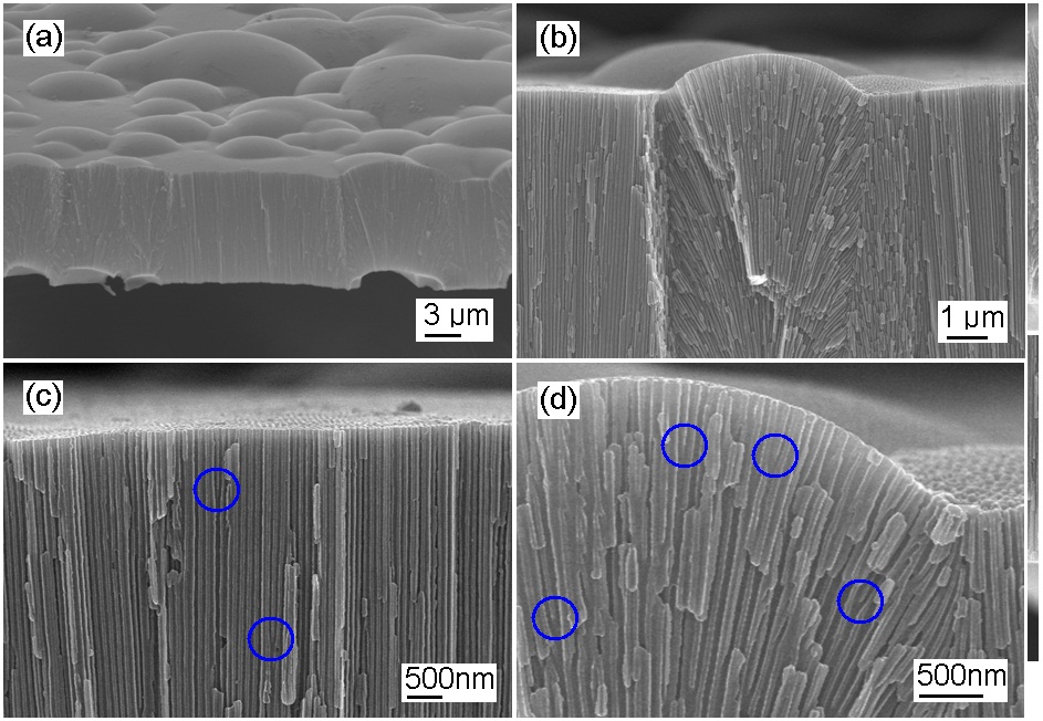
Figure 3 shows the SEM images of AAO after the removal of the barrier layer and the widening process. The upper surface with a convex lens-like shape is the counter-surface of AAO after the removal of the barrier layer and the pore widening process. The concave or crater-like initial surface influences the morphological formation of the convex-shaped Al/barrier interface. The total heights of the AAO layers are constant, whether the surface is flat or curved. For the curved surface, the AAO film showed a protruded cross-sectional image with a channel-limited cone shape in Fig. 3(b). A few split nanochannels are shown in a relatively flat surface area in Fig. 3(c), and there are many split nanochannels due to the severe surface distortion in Fig. 3(d).In the circled areas, there are split nanochannels where, for example,the equipotential curves show two minimal positions,so that a nanochannel can be split into two nanochannels. The nanochannel splitting can occur more in the curved surface region as shown in Fig. 3(d). The nanoporous AAO structure shows a relatively constant nanohole interval of about 101 nm and an average nanohole diameter of about 53.6 nm.
The formation mechanism of the nanoporous alumina in the anodization process is involved with the electric field-assisted processes of barrier formation and nanochannel dissolution[24]. The average radius of the porous cells is proportional to the applied voltage, and is approximately equal to the average thickness of the oxide barrier [25]. When we apply a constant voltage of 40 V to the anodic electrode on an Al plate, the current density drops suddenly [26], and the recovered current density then fluctuates periodically. When the current density drops, the insulating thickness of the 50 nm oxide barrier layer becomes a maximum, and provides an electric field of 0.8 × 10⁹ V/m.
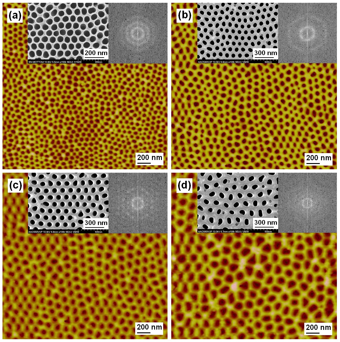
Figure 4 shows the atomic force microscope (AFM) and SEM images for the parameter change with various biases. The other process parameters of etching time, temperature, and density of the electrolyte solution are fixed. As the bias voltages increase to 30, 40, 50, and 60 V, the lattice intervals between the nanoholes increase to 79, 102, 120, and 156 nm, respectively. As shown in the insets, the periodicities were evaluated from the fast Fourier transform(FFT) analysis. The FFT patterns indicate that the nanoholes are arrayed with very low ordered structures of hexa-gonal lattices.The best hexagonal ordering occurred at a voltage of 40 V.
The optimal voltage for ordering indicates the physics on the charge screening at the interface of the Al metal and the ion solution. For the positively charged Al surface, the negatively charge ions or anions in electrolyte can be localized. The positively biased Al strongly attracts anions and also provide electrons to form Al ions. The strongly interacting electrons at the metal surface contribute to form surface plasmon states and can be diffracted to form the Friedel oscillation, causing the charge screening effect. The fluctuating surface charge density on the Al metal can be redistributed by the electric field, so that the interval between nanoholes is proportional to the field. Therefore,according to the charge diffraction pattern of Al metal, the ordering of hexagonal nanohole array of AAO can be formed on the interface between Al metal and AAO layer.
Furthermore, the charge diffraction pattern can be perturbed by the surface flatness. When the surface is not flat to a local curvature,the electric field is normal to the surface, and the curved surface adjusts the charge distribution. When two peak positions of the surface charge densities are overlapped due to the curved surface, the electric field attracts more of the electrolyte anions by forming a bigger hole than the other area. This phenomenon lowers the order of the nanohole array of AAO from the hexagonal lattice. Therefore, the order of the hole array and the uniformity of the hole size are influenced on the surface flatness correlated to the surface charge distribution.
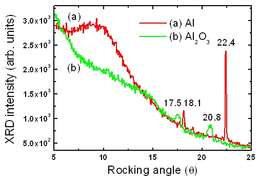
Figure 5 shows the X-ray diffraction spectrum of AAO before heat treatment. The structure of AAO is compared to the Al substrate.The Al metal shows peaks at the locking angles of 18.1° and 22.4°, which are different than the broad AAO peaks at the locking angles of 17.5°(311) and 20.8°(220). The AAO film shows a similar phase to crystalline γ-Al2O3. This indicates that the formation of the AAO nanopore structure comes from the electricfield induced reconstruction mechanism of the deposition and etching processes on the Al-O ionic bonds at the atomic level.
The electric field also acts as a driving force in diffusing anions into the Al/oxide interface from the surface. For a barrier that is thinner than the critical oxide thickness, the strong electric field can be applied on anions to be diffused into the interface, and the reaction occurs to form the oxide. After completing the formation of the oxide barrier, the pore formation can be started by lowering the formation energy. At the Al/oxide interface, the Al3 cation could not react to the O2- anion due to the limited diffusion process with the low driving force of the electric field on the anion for the critical thickness of the oxide. However, once the nanopores are formed, the nanopore structure lowers the critical electric field to form the porous AAO structure. The electric field can be concentrated on the edges of the holes and derive anions to be diffused into the Al/oxide interface.
As with the electric field covering the whole surface with a hexagonal unit cell, the inclusion of a new anion channel during the anodization process occurs for a region of a relatively enlarged area, and the hole edge shows a relatively broadened electric field distribution. The equipotential plane can also modify the circular distribution to be wide to a saddle point of dipole shape, and the charge diffraction can be modified so that the nanochannel can finally branch into two nanochannels.Furthermore, the new nanochannel can perturb the neighborhood so that the total porous structure can be formulated from the minimized energy. After the anodization process, the solution does not show an increased Al ion level, which indicates complete incorporation of the aluminum ion into the porous alumina.
We have investigated an anodization process for an Al surface with a curvature, and have demonstrated that the initial shape of the Al surface influences the order of the nanopore array,and branches the nanopore channel according to the electric field direction. For a surface with a very small variation of the Al surface, the channel branching is rarely occurred. However, for a distorted surface with a very high curvature, many new nanopores can be formed with the same diameters as the surface area increases under the uniform electric field. This branching effect of the nanochannel comes from the mechanism of the charge density oscillation at Al surface and the changed mode can cause the nanochannel branching in anodization process.