Graphene, which is a single sheet of carbon atoms in honeycomb lattice, is an emerging material to enable continuation of the scaling down of silicon based CMOS technology due to its special electrical properties [1-3], and the many efforts are being maded to realize graphene field effect transistors (FETs) with high performance. Since graphene is a zero band gap material with a linear energy-momentum dispersion relation, accordingly graphene FETs show a low ON-OFF current ratio of ~10 and a high OFF state current [4-7]. It is, therefore, required to open a band gap and lower the conductivity in order to achieve semiconducting properties. One way is to pattern the graphene into a narrow ribbon, which confines the carriers to a quasi onedimension.The energy band gap of graphene nanoribbon (GNR)depends on the width and orientation of the ribbon similarly to what happens with carbon nanotubes and a width of less than 10 nm can offer a sufficient energy bandgap to achieve the operation of a grapheme structure as an FET with a high ON-OFF current ratio [8,9]. In order to fabricate the fine GNR, top down lithography with an electron beam is carried out, and for pattern transfer, XR-1541 (hydrogen silsesquioxane) films, as a negative tone high-resolution electron beam lithography (EBL) resist, are used. Due to a high resistance tendency in the etching process,XR-1541 resists are difficult to remove after reactive ion etching(RIE). Also, XR-1541 films are known that have doping properties accompanying complementary n- and p-type doping when exposed by an electron beam. For these reasons, the existence of resist residues on the surface of graphene causes variations in the gating properties such as the shift of the Dirac point [10]. In this study, GNR is fabricated by EBL with XR-1541/poly methtyl methacrylate (PMMA) bi-layer resists and resist residues on the surface of GNR are successfully removed by way of a combination of the RIE process to cast away remaining PMMA/graphene films and the lift-off process to eliminate the XR-1541 resists. We developed a new process method which can increase the topgated dielectric properties with the removal of impurities on the GNR and expect to obtain many benefits in the production of integrated FET devices.
We prepared a silicon wafer with graphene films grown by the chemical vapor deposition method and transferred on SiO2 films with a thickness of 3,000 Å. The substrate was then spin-coated with PMMA electron beam resists with a thickness of 1,000 Åas a bottom layer and a XR-1541 negative resists of 500 Å thickness as a top layer. Nanoribbon patterns were fabricated by the XR-1541 resist with EBL writing (100 eKV; ELIONIX, ELS7000,Japan), and transferred to the bottom layer of the PMMA after development by the use of DPD-200D (DONG-JIN, Korea) and de-ionized water in a 3:1 ratio for 100 seconds. According to the etching barrier of the XR-1541 resist pattern, subsequent PMMA resists and graphene films are eliminated by the use of RIE (ICP380; Oxford, UK) with oxygen gas. In order to remove XR-1541/PMMA resists on the surface of the graphene channel,the specimen was dipped into dichloromethane, and then the lift-off process was carried out. Atomic force microscopy (AFM)and Raman spectra were measured and analyzed to identify the graphene structures.
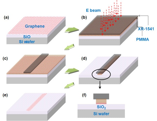
Figure 1 shows the schematics of fabrication for the graphene channel with EBL, using XR-1541/PMMA bi-layer resists. PMMA is coated on the graphene films, and XR-1541 is coated above in sequence. In terms of the XR-1541 resolution by bi-layer coating,it is proved that PMMA does not affect the contrast and the sensitivity of XR-1541 resists [11]. In a traditional single layer process with XR-1541, the fabrication of GNR for FET structures is not an appropriate process due to the following issues:
1) During RIE by oxygen etchant, both XR-1541 resists and graphene films are reacted and removed simultaneously. Moreover,SiO2 film used as an inter layer dielectric is etched by oxygen also.
2) Since XR-1541 resists contain an oxide group, H2SO4/H2O2 or HF-based chemicals are recommended for their removal.However, In this case, because graphene structures with carbon covalent bonding are also removed simultaneously by such chemicals, wet etching is not available in this process.
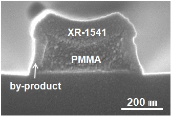
In order to deal with these problems, we tried out a lift-off process with bi-layer resists on the fabrication process of graphene FETs. PMMA, a conventional positive tone resist for the lift-off process and XR-1541 resists for pattern transfer are selected. At an initial attempt on the lift-off process after RIE, the XR-1541 resists were not lifted off well. In order to investigate the improper lift-off phenomenon, a specimen after RIE and the lift-off process is prepared and analyzed by scanning electron microscopy(SEM).
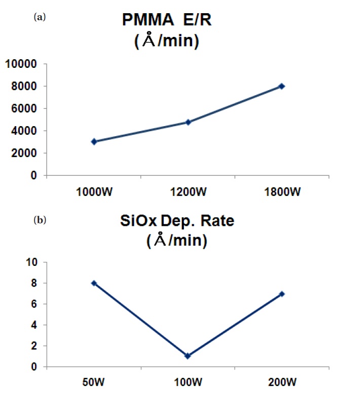
As shown in Fig. 2, the PMMA underneath the XR-1541 is not removed by the reaction with lift-off solvent. With additional etching for complete removal of graphene films after RIE, it is observed that the PMMA has reacted with SiO2 and re-deposited on the sidewalls of the PMMA. During PMMA/graphene etching,oxygen is used as a plasma gas. At this point, the major chemical component of the PMMA/graphene is carbon. So PMMA/graphene resists are etched by oxygen and by-products as CO2 gas are vaporized and pumped out. However, in the SiOx layer which appeared after graphene etching, the inclination of the deposition is a more dominant effect than the etching because SiOx bonding is easily broken due to the low ion bombardment of oxygen and recombination with Si and oxygen by means of an imperfect chemical reaction. The deposited thickness beforeand-after etching is measured by an ellipsometer. The deposited thickness of SiOx is 7 Å/min. At this rate, SiOx polymer is re-deposited on the sidewalls of the PMMA, and acts as an obstacle to the regular lift-off process. We optimized the etching parameters related bias and inductively couple plasma (ICP) so as to minimize the re-deposition rate of the SiOx which was added during additional over etching. Fluorine etchant gas can prevent the re-deposition of SiOx. However, at this point, the use of fluorine etchant is not effective on account of the decrease of the etching selectivity of the XR -1541 resists and the increase of the rate of SiOx loss. ICP Power is set at 1,800 W at the primary stage to minimize the degree of over etching, and then reduced to 1,200 W and 1,000 W in sequence. We fixed the ICP power as 1,000 W,the lowest power at which the plasma is stable at a pressure of 20 mT and measured the oxide deposition rate by changing the bias power from 200 W, 100 W, and to 50 W. The etching rate of the PMMA by ICP top power and SiOx deposition rate by bios power are shown in Fig. 3.
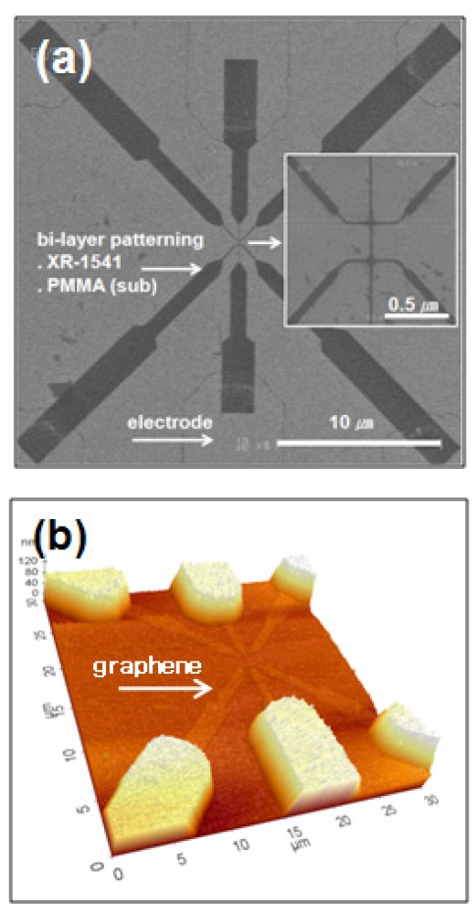
The measured oxide deposition rates are 7 Å/min at 200 W, 1Å/min at 100 W, and 8 Å/min at 50 W, respectively. The lowest deposition rate is optimized under the condition of 100 W of ICP power. The final parameter conditions of RIE for PMMA/graphene are a pressure of 20 mT, oxygen flow rate of 30 sccm, 1,000 W of ICP top power, and 100 W of bottom power at 40°C for 60 seconds. The SEM image after the EBL process and the AFM image of the GNR after the lift-off process are shown in Fig. 4.From Fig. 4(a), one can see that the GNR is oriented on the metal electrodes after applying the mix-and-match technique with EBL and an optical aligner. The resist pattern of XR-1541 performs the role of an etching barrier to plasma RIE. Under optimal RIE conditions, it can be seen that the lift-off process is accomplished and GNR remains well underneath the electrodes as shown in Fig. 4(b).
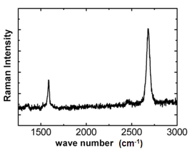
In order to identify the presence and electronic structure of graphene films, The Raman spectrum [12] is measured as shown in Fig. 5. From the Raman spectrum on the graphene channel obtained after RIE and the lift-off process, the two most intense features of the G and 2D peaks are shown at 1,583 cm-1 and 2,678 cm-1, respectively. This suggests that graphene has mono layer characteristics, which is verified by the fact that the ratio of I2D/IG is approximately 3 and the 2D peak has a symmetric shape.Also because no 2D peak is appeared at about 1,350 cm-1 it seems that the quality of graphene has been maintained without damage.
For fabrication of useful graphene electronic devices, further development of the fabrication process as well as synthesis techniques of high quality graphene are required. As a part of this process of improvement, we used top down lithography by utilizing EBL for the purpose of controlling the graphene band structure. To remove all resist residues which lie on the graphene channel, RIE and lift-off techniques with XR- 1541/PMMA bilayer resists were applied. Through the RIE and bi-layer process,GNRs were successfully finalized and demonstrated to have no damage. From these developments, we expect that the study of graphene- based FETs will become more accelerated.