The rapidly increasing use of transparent and conductive oxide (TCO) films for large-area displays and solar cells has prompted the development and study of inexpensive TCO materials, which exhibit appropriate optical and electrical properties. Recently, Ga doped ZnO (GZO) films have attracted attention, due to their high optical transmittance in the visible wavelength range, low electrical resistivity, and relatively low cost, compared to ITO thin films [1]. However, in GZO films, relatively high substrate temperatures are required, in order to simultaneously obtain the necessary electrical conductivity and optical transmittance in the visible wavelength region [2].
One way to improve the optical and electrical properties of TCO films without substrate heating is to use TCO/metal/TCO structures that have lower resistivity, compared to TCO single layer films of the same thickness [3-5]. In this study, transparent and conducting GZO films were deposited on Al coated glass substrate without intentional substrate heating, using DC and RF magnetron sputtering, and the effect of the Al buffer layer on the optical and electrical properties of the GZO films, and the optimal thickness of the Al buffer layer were investigated by UVvisible spectrometry, four-point probe measurement, X-ray diffraction (XRD), and atomic force microscopy (AFM).
GZO single layer and GZO/Al bi-layered films were deposited on glass substrate without intentional substrate heating by DC and RF magnetron sputtering, equipped with two cathodes. RF (13.56 MHz) and DC power were applied to the GZO (ZnO 95-Ga2O3 5 wt%, (purity: 99.95%) and Al (purity: 99.99%) targets,
[Table 1.] Deposition conditions of GZO and Al thin films.
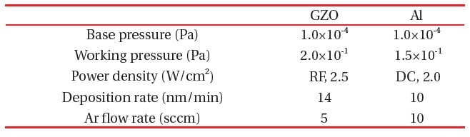
Deposition conditions of GZO and Al thin films.
respectively.
During deposition, the substrate temperature was monitored, using a K-type thermocouple in direct contact with the substrate surface and was maintained at 60℃. Prior to deposition, the chamber was evacuated to a pressure of 7×10⁻⁷ Torr. Sputtering was performed at 1×10⁻³ Torr in argon (Ar) and the deposition distance between the target and substrate was maintained at 6 cm. By controlling the deposition time and sputtering power, the thickness of GZO film was maintained at 100 nm, while the thickness of the Al buffer layer was set at 2 and 5 nm, respectively. For comparison, 100 nm thick GZO single layer films were also deposited, under the same deposition conditions. Table 1 shows the deposition conditions of this study.
After deposition, the crystallization of the films was observed with high resolution X-ray diffraction (XRD, X’-pert Pro MRD, Philips, at the Korea Basic Science Institute, Daegu Center) and the grain size was also evaluated with Scherrer equation [6]. The root mean square (RMS) roughness was analyzed using atomic force microscopy (AFM, XE-100, Park Systems). In addition, optical and electrical properties were assessed using four-point probe measurement and a UV-Vis. Spectrophotometer (Cary 100 Cone, Varian), respectively. The glass substrates showed 90% optical transmittance in the visible wavelength range. The performance of the GZO single layer and GZO/Al bi-layered films as transparent conducting films was evaluated using the figure of merit (FOM) [7].
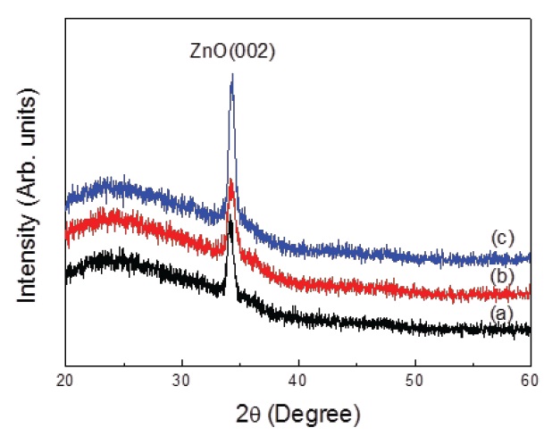
In order to evaluate the optical and electrical performance of GZO/Al bi-layered films, structural characterization is very important, because the optical and electrical properties of the films are strongly dependent on the microstructure. Figure 1 shows the XRD patterns of GZO single layer films and GZO/Al bi-layered films. For all of the films, the diffraction peak in the XRD pattern was identified as ZnO (002) plane. Although the Al underlayer did not show any diffraction peak in the pattern, it is supposed that the Al underlayer may enhance the crystallization of GZO films, because the full width at half maximum (FWHM) of the ZnO(002) peak deceased proportionally with the Al thickness [6].
Table 2 shows the grain size of the GZO single layer films and GZO/Al bi-layered films. With increased thickness of the Al underlayer, the grain size also increased up to 30 nm, in GZO 100 nm/Al 5 nm films. In a previous study, Y. Kim reported similar results that in ITO/Au bi-layered films, the crystallization of the ITO film is also promoted by the Au underlayer [8].
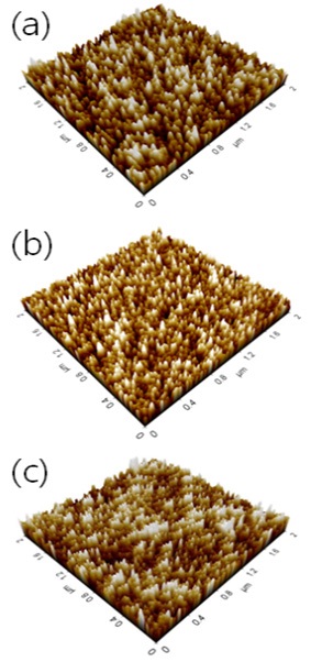
The surface roughness of TCO films is a critical factor, especially for applications in OLEDs. Because the thickness between the anode and cathode in OLED devices is several hundred nanometers, it is critical that the film surface be smooth, to ensure the performance of the OLED devices [9].
Figure 2 shows AFM images (2×2 μm2) of the as deposited GZO and GZO/Al films. The RMS roughness of the as deposited GZO film was 2.4 nm, and with increase of the thickness of the Al
[Table 2.] Grain size of GZO and GZO/Al films with different Al thickness of 2 and 5 nm.
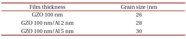
Grain size of GZO and GZO/Al films with different Al thickness of 2 and 5 nm.
underlayer, the RMS roughness of the films was decreased. The lower RMS roughness of 2.0 nm was obtained from the GZO 100 nm/Al 5 nm bi-layered films. Based on the AFM images, it can be concluded that the thin Al underlayer may enhance the surface flatness of GZO films.
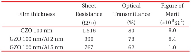
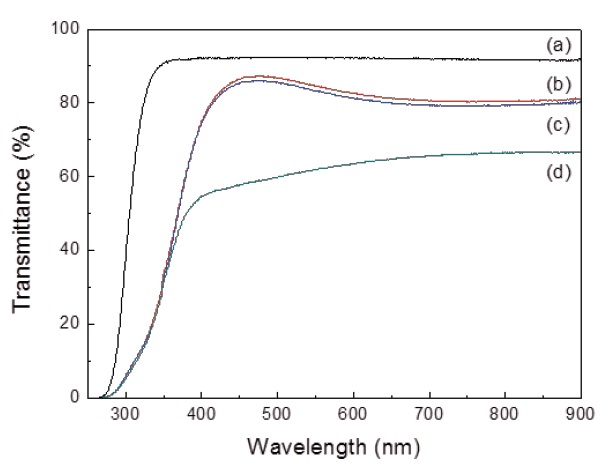
Figure 3 shows the optical transmittance for the wavelength range of 300-900 nm. The GZO films show an optical transmittance of 80% in the visible wavelength region, and with increase of the thickness of the Al underlayer, the optical transmittance of the films was decreased. The GZO 100 nm/Al 2 nm and GZO 100 nm/Al 5 nm films show lower optical transmittances of 78% and 62%, respectively, than those of the GZO single layer films. As shown in Fig. 3, the optical transmittance was decreased as the thickness of the Al underlayer increased, because the metallic Al layer may absorb visible light [10]. Thus, although the metal underlayer may reduce the electrical resistivity of the films due to enormous carrier density, its high optical absorption is a drawback that limitsal transmittance of TCO films. In order to obtain high quality GZO/Al films, the thickness of the Al underlayer should be optimized. The Fig. of Merit (FOM) is an important index for evaluating the performance of TCO films [7]. The FOM is defined as FOM = T10/Rs, where T is the optical transmittance in the visible wavelength region and Rs is the sheet resistance. Table 3 optical and electrical properties of the films. While the optical transmittance of GZO films is deteriorated with the Al buffer layer, the GZO/Al films had a lower sheet resistance compared to that of the GZO single layer films. In Table 3, the FOM reached a maximum of 8.4×10⁻⁵ Ω-1 for the GZO 100 nm /Al 2 nm films, which is higher than the FOM for the GZO single layer films.
Both GZO single layer and GZO/Al bi-layered films were deposited on glass substrates, using DC and RF magnetron sputtering.

A comparison of optical and electrical properties of GZO single layer and GZO /Al bi-layered films with different thickness of Al underlayer.
The optical and electrical properties were dependent on the Al buffer layer in the GZO/Al films. Figure of Merit (FOM) for the GZO 100 nm/Al 2 nm films reached a maximum value of 8.4×10⁻⁵ Ω-1, which is higher than that of the GZO single layer films. Since the higher FOM value indicates better performance of TCO films, it is supposed that the GZO films with 2 nm thick Al buffer layers will likely perform better in TCO applications than GZO single layer films.