Reverse engineering has been utilized to analyze the layer structure and materials in a semiconductor device, to identify the cause of device failure, or to apprehend how the circuits are constructed. Layer extraction processes are the key technique in reverse engineering; these include delayering or etching of metal interconnection lines, passive components, and dielectric films stacked over the poly-silicon gates of a transistor [1]. As semiconductor device sizes are shrinking for high performance and high density, Al metal lines have been replaced by Cu metal, to reduce interconnection resistances. In addition, Cu via-plugs are also used for vertical integration in submicron devices [2]. These advanced technologies make the delayering processes more difficult, because of the complexity in layer structures. For Cu metal etch, most researchers have employed plasma-based etch techniques, using chloride or oxidizing agents [3-5]. The well-known Cu interconnection processes, i.e. (dual)-damascence processes, have avoided metal etch, and employed chemical mechanical polishing to remove excess Cu layers at the end of via-plug formations [2,6,7]. Relatively few studies are reported on the wet chemical etch of Cu metal layers [8]. Therefore, delayering processes of Cu metal lines formed in the trench of dielectric films need to be developed, without damaging the vertical plug-via structure, and surrounding inter-metal dielectrics. In this study, the delayering processes of Cu interconnected semiconductor devices are investigated, to exhibit how the circuits are designed, to reconstruct the circuit layouts for reverse engineering.
Reverse engineering starts with the cross-sectional examination of a specimen, to monitor the number of metal layers, elements of metal, thickness and composition of inter-metal dielectrics, etc. We employed a scanning- (SEM) and transmission(TEM)
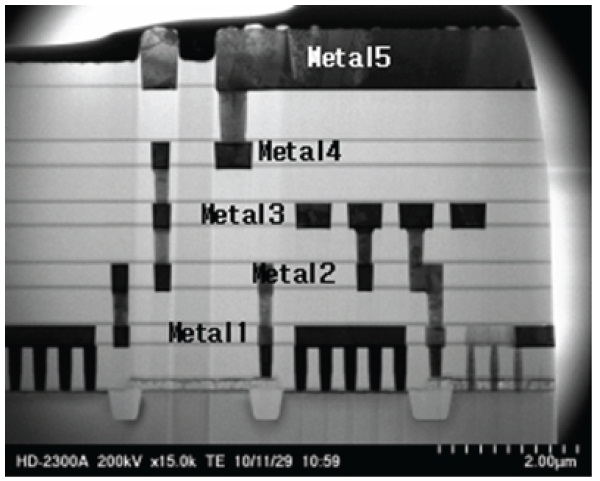
electron microscopy for the examination. The specimen used in this study was composed of five metal layers separated by SiO2 dielectrics, and the vertical interconnections were made of Cu. Barrier metals for Cu via-plugs were not closely analyzed, but commonly used TiN was presumed. The result of a crosssectional SEM image of a sample is displayed in Fig. 1. From this, we obtained a Cu/Ta metal layer thickness of 800 nm/30 nm, 300 nm/20 nm, and 220 nm/20 nm for Metal 5, Metal 1~4, and Metal 1, respectively. Gate poly-Si was 140 nm thick. The dielectric film thickness was 450 nm between Metal 1 and 4, and became thicker, to be 600 nm over the poly-gate and 700 nm under the Metal 5.
As the cross-sectional view of an IC does not provide how other passive components - capacitor, inductors, and resistors - are connected with underlying gates, planar layouts have to be disclosed after layer-by-layer removal. The removal of capping layers composed of molding compounds was accomplished by sulfuric acid, fuming nitric or sulfuric acid [1]. Once the molding compounds were dissolved, the protection layers deposited in IC fabrication processes were exposed, which were usually comprised of SiOx, SiNx, or in some case polyimides. These layers were removed by the dry etch method, using reactive ion gases excited by RF plasma in a Samco RIE 10NR; as a result, top metal interconnection lines were exposed. As the metal lines are constructed not only laterally but also vertically through dielectrics, the delayering process should reveal vertical via-plug patterns, after disintegrating the planar Cu lines. We have tried wet chemical etch, dry etch, or mechanical polishing to remove the top Cu metal layers labeled “Metal 5” in Fig. 1, without damaging much of the via-plug structures.
After top metal along with a part of the via-plugs was etched away, mechanical polishing was utilized to flatten the surface, and to eradicate Cu remains. At this stage, the locations of vertical interconnection were recognized. The surrounding intermetal dielectrics (IMD) were removed by dry etch, using a reactive ion etcher (RIE), then the patterns of under-lying metal line were exposed. Metal etch and mechanical polishing followed by plasma etching of IMD layers were repeated for other remaining multiple layers, until the final gate level connections were revealed.
At the end of the decapsulation step, a dark brown or apricot colored passivation surface was shown. In some devices
[Table 1.] Reactive ion etch conditions for the passivation layers.
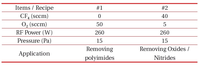
Reactive ion etch conditions for the passivation layers.
we studied, the polyimide layers were additionally deposited over SiOx or SiNx film. These protection layers can be removed, either by chemical etching, or by plasma reactive ion etching. The well-known chemical etchant for SiOx was buffered-oxideetchant( BOE) which has good etch selectivity for most metal/ oxides, but had the drawback of etching W via-plugs in our findings; thus, we never attempted to use it for Cu via-plug samples. On the other hand, reactive ion etching exhibited an advantage, with faster etch speed and uniform etch rate over the entire surface. Numerous ratios of CF4, O2, Ar gas were tested to obtain the optimum condition, and the best results were obtained under the isotropic etch conditions as follows: O2 only for polyimide, and the mixture of CF4/O2 for SiOx and SiNx. The detailed conditions are summarized in Table 1. It should be noted that removing polyimide required sample cooling, to avoid carbonized residues on the surface. The typical etch rate of polyimide, SiOx, and SiNx showed 1 ㎛/min, 150 nm/min, and 200 nm/min, respectively.
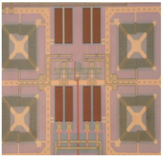
When the passivation layer was completely removed, the surface turned to dark orange color, which is an indicator of Cu metal surface. It was important that etch time should be carefully controlled, to reveal the same color tone over the area under a microscope. The top metal patterns are displayed in Fig. 2.
Next step was the relayering of top Cu metal (“Metal 5”) lines; several methods have been exercised to obtain a clear surface morphology, without damaging via-plugs. Firstly, we utilized the reactive ion etch with Ar gas at an anisotropic etch condition. However, the etch rate of Cu was too slow to finish the process within 1 hr for normal Cu thickness, even at high Ar flow rate, high plasma power, and low operation pressure. Secondly, mechanical polishing with 0.05 ㎛ fine alumina powder was employed, because the film grinding rate can be controlled by the applied force, speed, types of cloth, etc. However, the polishing was not selective between planar Cu lines and vertical Cu viaplugs, but also removed near-edge area faster than in the cen-
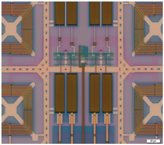
ter, so that we often found via-plugs disappear near the edges. Thirdly, we used concentrated poly-Si etchant: a mixture of hydrofluoric acid, nitric acid, and acetic acid (1:4:20). Although all exposed Cu lines were rapidly etched away within 10 sec, the etchant also attacked some of the Cu via-plugs, and penetrated down to the lower Cu lines. Once this local over-etch happened, it became worse during further processes, leading to a failure of reverse engineering. In contrast, when poly-Si etchant was diluted in water (1 part of etchant in 3 part of water), the planar Cu layers were etched nicely, without aggressive via-plugs damage. The etch rate of Cu for this diluted solution was as low as 15 nm/ min; thus, the process time can be controlled, to avoid excessive via-plug etch. We also found that this etchant dissolved TiN, Ta, and Ti barrier layers. Figure 3 displays the results, after Cu metal lines were removed.
After the top metal layers were etched away, mechanical polishing at a rotation speed of 100 rpm using 0.05 ㎛ alumina powder was effective in eliminating the remaining Cu residues, and flattening the surface. When the film was ground by 100~200 nm, the round shaped Cu via-plugs were nicely revealed in the background of dielectric film on a microscope, which informed us where the vertical interconnections were made.
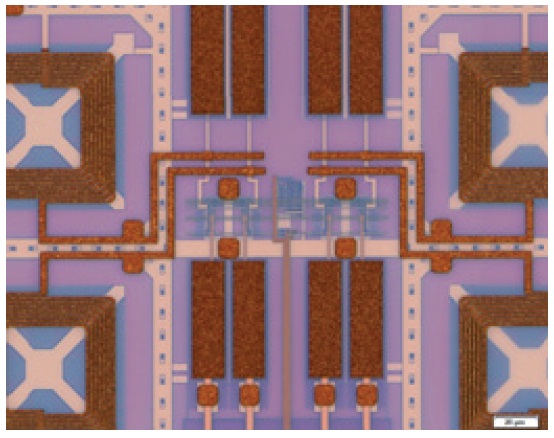
In order to recognize the underlying metal (“Metal 4”) patterns, the IMD layers have to be disintegrated. We employed CF4/ O2 plasma etch at various test conditions, by changing the CF4 flow rate from 5~35 sccm, O2 flow rate 0~15 sccm, and RF power 50~300 W. The best morphology of via-plugs over the 2nd metal lines was obtained at the condition: CF4 flow rate of 25 sccm, O2 flow rate of 0 sccm, pressure at 3 Pa, and RF power at 200 W. This etch condition was slightly different from the recipe employed for the passivation layer removal, and it induced more anisotropic, in other words vertical etch. The etch rate of SiOx was about 50 nm/min at the optimum condition. Even though the conditions were optimized, there remained some dielectrics at the sidewalls of via-plug pillars. Care was taken not to peel off the underlying 2nd metal layers by over-process. Short mechanical polishing was followed, to remove via-plugs, sidewall remains, and to flatten the top surface. At the end of this stage, the patterns of underlying Cu metal lines, as displayed in Fig. 4, were recorded by a scanning electron microscope. We further resumed the metal etch, followed by mechanical polishing, and RIE dry
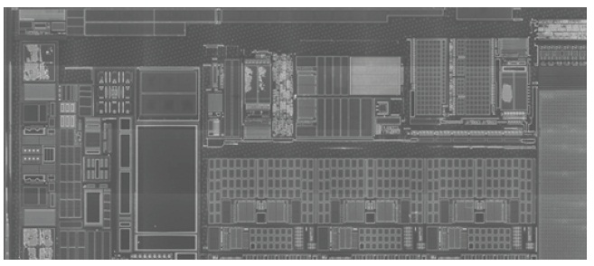
[Fig. 5.] A reconstructed image of the poly-Si pattern out of 600 photos at the end of deprocessing.
etch of dielectric layers, until the poly-Si layers over a transistor were exposed.
At the end of each step of layer removal process, high magnification SEM images (4,000X) were collected. These local images, taken from 50~600 spots dependent on resolution, were combined to make one global view corresponding to each metal layer, utilizing a built-in “analySIS TS Auto” program. Thus, we were able to obtain a whole view of the metal patterns, and the final image of poly-Si patterns over transistors is shown in Fig. 5 as an example. These images were delivered to a circuit analysis engineer, for the next step organization of circuit layouts.
The delayering of a Cu interconnected Si device is explored for the reverse engineering of an IC. After decapsulation of the molding compounds, the passivation layers were removed, by using CF4/O2 gas mixture under the isotropic plasma reactive ion etching condition. When the Cu metal was exposed, we utilized the diluted poly-Si etchant, 1 part of the etchant (1 HF:4 HNO3: 20 CH3COOH) in 3 parts of water, to etch the Cu planar metal lines, and a part of the Cu via-plugs. The wet-etch rate was as slow as 15 nm/min; this mixed solution resulted in reliable data from numerous samples. Mechanical polishing then followed, to flatten the surface, and to reveal the via-plug locations. The surrounding IMD layers were delineated by using CF4 gas only at low pressure, to provide an anisotropic etch condition in a reactive ion etcher, and the etch rate of about 50 nm/min. After the dielectric layer disintegration, the Cu metal lines was exposed, and the metal etch was repeated again with the wet etchant, until the final poly-gate patterns were displayed. Finally, the recorded local views of metal pattern, via-plug, and passive element were reconstructed, to provide a grand view of the interconnection schemes of each metal layer. This procedure would provide the annotations of circuit layouts for a reverse engineer.