The trend for digital and analog integrated circuits (ICs) is to perform with a higher integration and frequency. This promotes a more advanced technology for electronic devices and makes daily life more convenient. The decrease in geometry length induces a reduction in power supply voltage and, consequently, noise margin. The prediction of electromagnetic immunity is a pivotal issue for high speed and high frequency ICs. The immunity of ICs is crucial for the performance of related electronic devices, and even for the functioning of entire operating system. Much research on estimation of immunity for ICs has been published in [1-6]. These papers cover a systematic discussion from modeling to measurement for the estimation of immunity of ICs. A summary of the electromagnetic compatibility of ICs was proposed in [7], and immunity was addressed in that paper.
Several measurement methods have been published by the International Electrotechnical Commission (IEC) to characterize the behavior of ICs in response to electromagnetic interference. One of these methods is direct power injection (DPI) [8]. The conducted immunity of ICs can also be predicted based on the bulk current injection (BCI) method defined in the IEC 62132-3 standard [9].
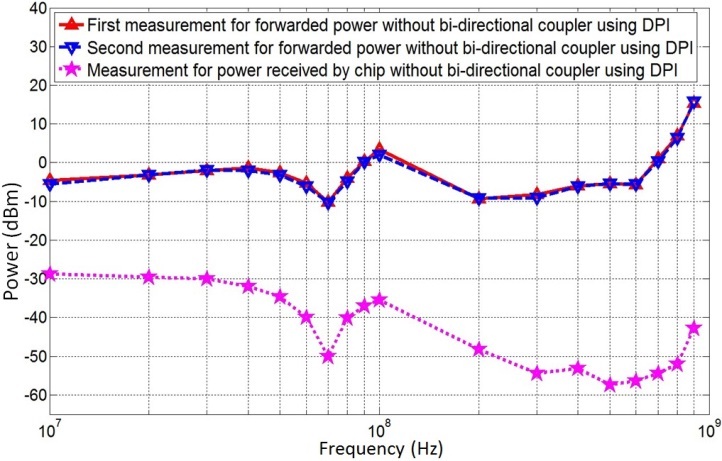
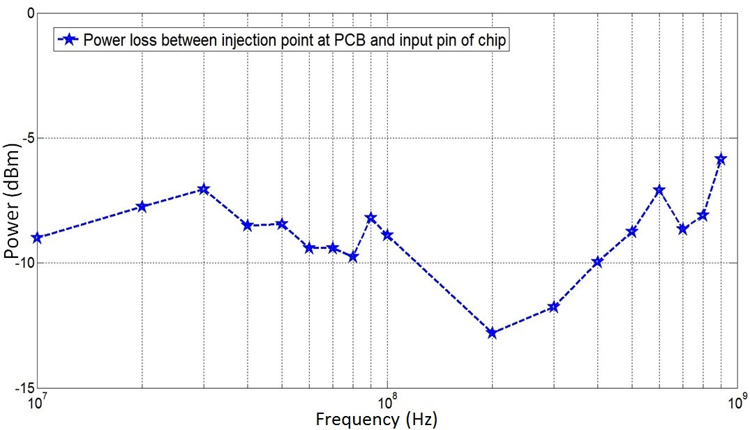
However, the forwarded power, which is regarded as the immunity index in these criteria, is not the real tolerable power of the ICs since an obvious power loss between the forwarded power and the power received by the chip. This power gap phenomenon has been demonstrated in [10], and is shown in Fig. 1. The magnitude of the chip received power reflects the practical level of tolerable noise for the ICs. A more precise immunity for ICs based on the power received by the ICs needs to be defined and extracted. This requires an analysis of the power gap, as well as a new method for extracting the real immunity.
The DPI and BCI test approaches divide the power transfer network into two parts: an external off-board equipment block and the printed circuit board (PCB)-packagechip power distribution network. Power transmits through a cable as a simple trace in the outside setup and the route of power propagation in the latter network seems complicated and more significant. A well designed power trace avoids undesired power loss and fluctuation when the power supply system experiences interference from internal and external noise. The immunity criterion can be extended from the injection point of the PCB, which is regarded as the measurement site for the forwarded power to, the input pin of the chip for complete power loss analysis of the power distribution network between the PCB and the chip.
This paper proposes a novel algorithm to extract a more accurate immunity of integrated circuits based on the implementation of the power transfer function. In Section Ⅱ, the fundamental theory of the power transfer function is explained and parameters related to the power transfer function in a DPI test system are also described. Section Ⅲ discusses our design power propagation route for continuous wave or impulse wave noise injection experiments, and identifies the source of power loss in this trace. A two-tier calibration method is applied to extract the scattering parameters for the designed power transmission path, and finally obtains the power transfer function for it in Section Ⅳ. Therefore, the real immunity of the chip located in our designed platform is obtained.
Ⅱ. FUNDAMENTAL THEORY OF THE POWER TRANSFER FUNCTION
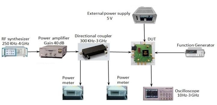
As we mentioned in Section I, the DPI method is app-ropriate for immunity prediction for a power distribution network. The typical measurement setup for the DPI method is depicted in Fig. 2.
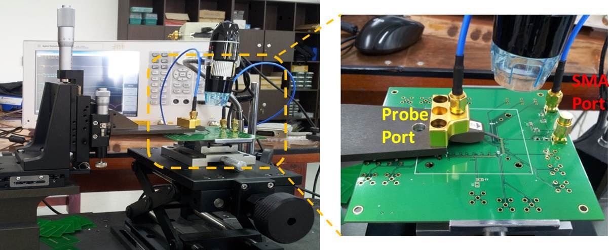
A chip, as a victim of direct power injection in the electromagnetic susceptibility (EMS) test, has been designed and fabricated using 0.18 μm CMOS technology; it consists of a 4.5 mm×4.0mm chip with outer 80 pins thin quad flat patch package. It is mounted on a specially designed 4-layer PCB platform that includes multifunction SMA ports for the DPI test.
The characterization of the immunity of ICs as an index of the tolerable power accepted by the circuits is a target of the DPI test. However, factors such as impedance mismatch and radiated emission cause a reflection of most of the radio frequency (RF) power delivered by the generator, and only a small amount enters the IC under the test conditions. Consequently, the efficiency of the transmitted power must be computed.
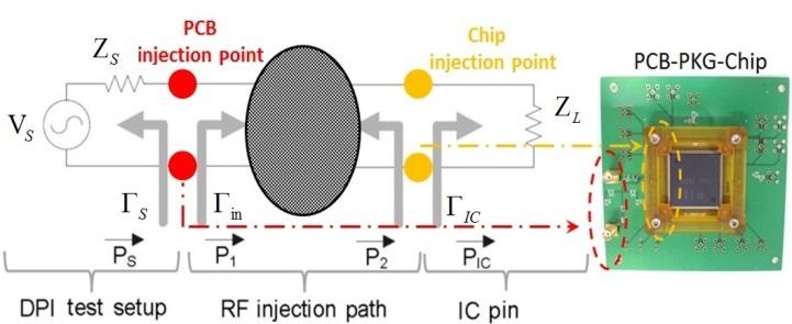
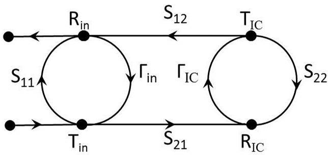
The power loss between equipment outside of the PCB is negligible compared to the noise power level, so the analysis of power loss in the DPI experiment focused only on the PCB-package-chip system. The equivalent circuit block for the DPI setup is described in Fig. 3. It includes three sections from the source to the chip, an external setup, an RF injection path and the chip. Reflection occurs when power arrives at the boundary of two near sections due to impedance mismatch. Reflection coefficients are used to express the degree of mismatch and the transfer efficiency at that specific injection point. They are the
The reflection coefficients are the pivotal factors for the transfer function of the power network. The transfer function of the network from the injection point at PCB to the pin of the chip is defined as the ratio of the power received by the load and the injection power, which is shown as Eq. (1). The power injected into the PCB and the power received by the chip are represented by the voltage and characteristics of the two-port network, as described in Eqs. (2) and (3). The derivation of the function can be referred to [11-13].
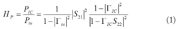
These equations show that the power transfer function relies on the reflection coefficients at the injection point and the IC pin. Furthermore, the scattering parameter of the intermediate system has a significant effect on the final result of the power transfer function. The two port network between the injection point and chip pin is transferred into a signal flow chart in Fig. 4 for a derivation of these reflection coefficients.
In Fig. 4, the symbols T and R are the expressions of the transmitted and reflected wave. The
The impedance of the output port for the RF signal generator and power amplifier is 50 Ω, and it equals the power cable impedance. A negligible or even no reflection situation results for the reflection coefficient at the source. This simplifies
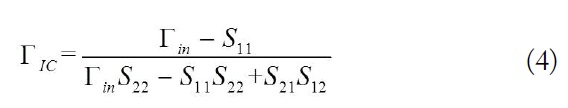
Normally, the reflection coefficient at the injection port of PCB is easier to measure than that located at the input pin of the chip. A more applicable equation for the power transfer function extraction generated in Eq. (4) on the basis of the equations in [11-13] is:
The power transfer function with only an unknown and a scattering parameter is obtained after substituting (4) into (1). The reflection coefficient at the injection port of PCB
Ⅲ. DESCRIPTION OF THE DESIGNED POWER TRANSFER TRACE
The goal of the power transfer trace is to effectively and safely lead the RF injection power to the ICs. In the standardized test approach, the RF noise is injected into the DC power supply system. The RF generator or power amplifier might be influenced by the DC power. Establishment of a separation or block circuit between the RF and DC loops is therefore necessary for a protection effect.
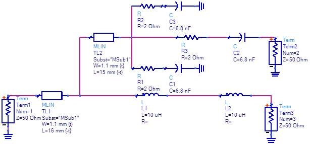
A designed circuit used as a coupled path for an AC and a DC signal is proposed in Fig. 5. An AC decoupling network is placed between the RF noise path and DC power supply to avoid a DC power feedback to the sensitive RF equipment.
The decoupling network consists of three parallel 2 Ω resistor and 6.8 nF capacitor pairs that can tolerate an impulse noise, thus making the designed circuit compatible with both continuous and pulse wave injection tests. The RF inductors located in the DC path ensure a single directional transmission of an RF noise to the chip, and avoid any influence on the DC supply device.
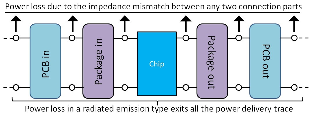
In any designed power transfer traces, impedance match cannot be achieved perfectly, and power radiation also exists. Therefore, they are the cause of the power loss phenomenon, and a well-designed power delivery network could improve the power transmission efficiency, and obtain the maxim injection effect. The power loss description for an RF injection system is depicted in Fig. 6. The most power loss would happen at the boundary between the board and package or the package and chip due to the impedance mismatch, while power losses of less than 0.03 dBm are detected between the board and the external equipment connection in our test. In the high frequency range, a transmission line on board might act as an antenna, and therefore generate radiated power losses to reduce the power transfer efficiency.
Ⅳ. DERIVATION OF THE POWER TRANSFER FUNCTION BASED ON MEASUREMENT
As mentioned in Section II, the reflection coefficient at the injection port of board and the scattering parameter of the mixed two-port network determine the final power transfer function. In this section, extraction of and the scattering parameter based on a one-port measurement and a two-tier calibration is addressed.
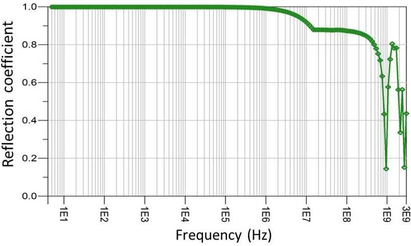
The one-port measurement simulates the reflection phenomenon in the real injection situation. The RF noise enters the board through the SMA type port where the reflection happens. Another port is terminated with 50 Ω impedance since it is connected to a DC power cable that has 50 Ω as its characteristic impedance in the IEC standardized test. The measured reflection coefficient at the input of the RF noise injection path is shown in Fig. 7.
The reflection coefficient approaches 1 at the DC frequency range and gradually declines with a growing of the frequency. As an RF propagation trace, the DC power is mostly blocked and only transmits the high frequency signal based on the measured reflection coefficient. The reflection coefficient is sensitive to the port impedance and scattering parameters of the network. Even a small variation in these variances would result in a significant effect on the reflection coefficient.
Scattering parameter measurement of the power delivery network at a PCB is a challenge since the two ports are of different types. One of the ports can be measured with a probe, while the other port matches the SMA connector type. This unbalanced situation for the two ports results an error that is not negligible in the calibration stage. Thus, a technique to eliminate the calibration error is required for an accurate S-parameter test. Here, we introduce a two-tier calibration to fulfill the target. In the two-tier calibration method, a renormalization technique is developed to extract the real scattering parameters
The procedure of a two-tier calibration method is as follows:
1. One-port calibration of the SMA type port using an E-calibration or manual calibration kit.
2. One-port calibration of the input pin of the chip using a probe and the corresponding substrate kit.
3. Implementation of a two-tier calibration deviation correction system to remove the unbalance errors.
4. Measurement of the scattering parameter of the mixed two-port network.
Each one-port calibration result is sent to the vector network analyzer in step 1 and step 2. However, the transmission characteristics of the two ports are not checked in these two one-port in two times one-port calibrations. A deviation correction system is applied to receive the calibration result generated in step 2. A modification of the preliminary result is then carried out in the system to make the result in step 2 compatible with the calibration outcome in step 1; this leads to a better transmission characteristic for the two ports. At this point, the two-tier calibration has been completed, and a test of the S-parameter can now be performed.
After the two-tier calibration, the unbalance error has been eliminated and the insertion loss of the two-port is nearly 0 dB. It is appropriate to take a measurement under this condition, and a figure to describe the two-tier measurement is shown in Fig. 8.
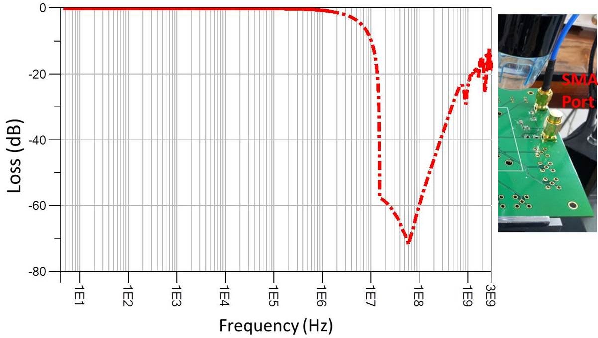
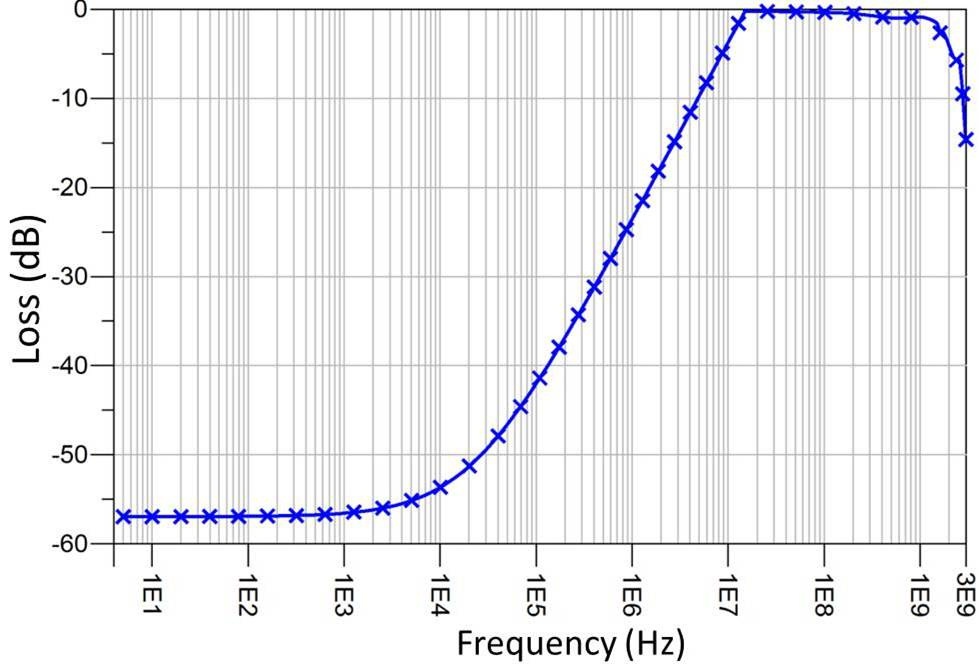
The power transfer network has a pair of two-port systems. One of them is the RF noise transmission trace and the other is the DC power supply path. They both include the output port, which is an input pin of chips, and are distinguished by the input port as an RF injection or DC supply. The insertion loss for the DC power propagation and RF noise paths is measured and shown in Figs. 9 and 10 to validate the designed power transmission network.
In Figs. 9 and 10, the insertion loss of the DC power supply shows a good transmission property at low frequency, while the insertion loss of the RF noise path transmits the signal well at high frequency. The former one works as an AC block and the latter one performs a DC block characteristic to protect them both.
At this point, all required parameters for extracting the power transfer function come out, and then parameters are substituted into (2) - (4) to derive the power transfer function in (1).
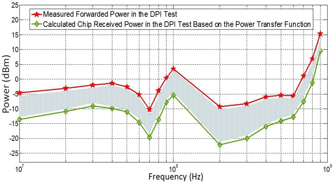
Once the power transfer function of the injection network is known, the power gap between a forwarded power and a chip received power can be calculated based on the transmitted power magnitude and shown in Fig. 11. As described in this figure, the chip received power is not the forwarded power, which is defined as the immunity criterion in the IEC 62132-4 standard since power loss occurs between them. Thus, the immunity index determined as the maximum tolerable power by chip should be corrected as the chip received power rather than the forwarded power. A more accurate tolerable power level at the chip stage is achieved and it is obviously lower than that of the forwarded power due to the power loss in the transmission path. A comparison of two immunity levels based on forwarded power and chip received power is shown in Fig. 12. The difference in the immunity level as the shadow section shown in Fig. 12 is a sensitive range and has a profound effect on accurate immunity prediction of ICs.
In a real application, the platforms as a package or a board for a chip have different power losses from power input at the edge of the board to the output as an input pin of a chip. The power gaps vary in different designed packages and boards. In the DPI test standard, immunity is defined as the maxim tolerable forward power for a specific IC, while the chip received power might change substantially with another board or package in a real application. A malfunction or even damage can easily occur if the criterion of immunity standards still refers to the forward power as defined in the IEC standard.
As a result, an implementation of the novel proposed immunity criterion would avoid these types of accidents in actual situations.
In this paper, we proposed an accurate approach for predicting the immunity of ICs based on the power transfer function. A two-tier calibration method is developed to measure the scattering parameter of a mixed two-port power transmission network at the PCB. The reflection coefficient is also obtained based on one-port measurement. The power transfer function is finally achieved and a more precise immunity is extracted than the immunity based on the IEC standardized DPI method. The immunity estimated by our proposed method approaches the real tolerable power of ICs and has a significant effect on immunity prediction for any platform of ICs in a real implementation.