Technological developments in the super minimal electronic device industry have led to miniaturization of expensive devices, such as semiconductors and memory chips. These devices are illegally used as hidden devices containing industrial information including top secret data. The methods used to hide these illegal devices are often skillful and ingenious, so that detection is becoming increasingly difficult. A wireless non-linear junction detector (NLJD) with high performance has been studied as one method for detection of a hidden device [1]. This has introduced a need for a high gain antenna that can detect hidden devices, had been raised. High performance NLJD systems as well as broadband antennas with high gain are now being studied in many countries, including Korea [2]. For example, a hidden device composed of a semiconductor is easily detected by the amplitude signal level received by a NLJD, because the 2nd harmonic amplitude of a hidden device that is a pure semiconductor is higher than the amplitude level of the 3rd harmonic frequency. On the other hand, a false junction material composed of a semiconductor and a metal has a 3rd harmonic amplitude level that is higher than the 2nd harmonic amplitude. These harmonic amplitude differences allow easy detection of a hidden device. This phenomenon is theoretically derived by the analysis of the semiconductor currentvoltage (I-V) equation using the Fourier transform. The NLJD antenna has to satisfy the transmitting frequency (Tx) band and the receiving frequency (Rx) band simultaneously, so a wideband antenna is required for the NLJD [3].
The circular polarization (CP) antenna has been mainly used for the NLJD system applications because of its high capability for recognizing and detecting hidden devices [3]. The CP pattern of a proposed circular disc patch antenna has been applied and designed by a truncated corner structure of a ground plane [4,5] with 45° inclined slots [5], two rectangular grooves on the circular disc patch [6] and an asymmetric gap at the feeding structure. Sections Ⅱ and Ⅲ present a theoretical analysis of the frequency response characteristics for the NLJD system and a novel design for wideband circular patch antenna, respectively. The linear array design of 2×1 is considered to increase the gain as described in Section Ⅳ. In Section Ⅴ, a proposed antenna for single element and two element arrays was fabricated and measured. The measured and simulated results are discussed and compared.
Ⅱ. THEORETICAL ANALYSIS OF HIDDEN DEVICE DETECTION
The harmonic response difference between the semiconductor and the false junction results from a non-linear I?V equation. The I?V equation of semiconductor is as follows [7].
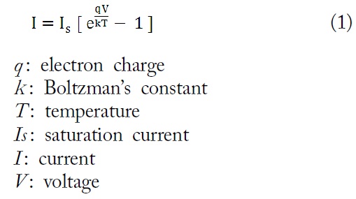
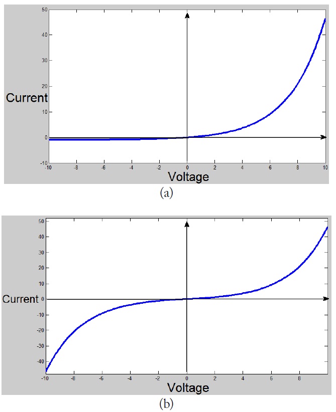
The I?V of the semiconductor and the false junction is calculated by Eq. (1). Fig. 1(a) and (b) show the I?V characteristics of the semiconductor and the false junction, respectively. The I V characteristics of semiconductor shown in Fig. 1(a) are similar to an exponential graph. Those of the false junction, shown in Fig. 1(b), are similar to a tangential graph. For example, the I?V equation of the false junction is derived and analyzed by current with respect to voltage response of the forward-reverse bias of the two zener diodes. The false junction has the symmetric voltage characteristics as shown in Fig. 1(b). A non-linear device has special characteristics having harmonic components for an input of the frequency. These harmonic characteristics give the semiconductor and the false junction different harmonic amplitude levels. A Fourier transform is employed for transformation of the frequency domain with respect to the time domain. The frequency domain for Fig. 1 is expressed using the Fourier transform as follow [8]:

In Eq. (1), when
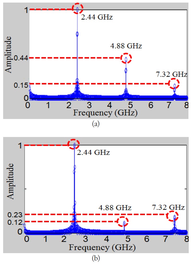
The relative amplitude of the false junction in the frequency domain is 1 at 2.44 GHz, 0.2 at 4.88 GHz and 0.39 at 7.32 GHz, as shown in Fig. 2(b). The false junction calculation shows that the 3rd harmonic amplitude level is higher than the 2nd harmonic amplitude, as shown in Fig. 2 (b). Therefore, the hidden device is simply detected by the difference in harmonic response.
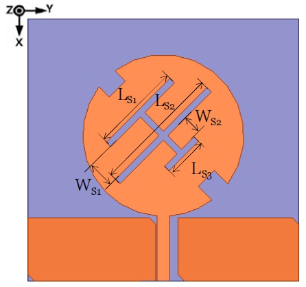
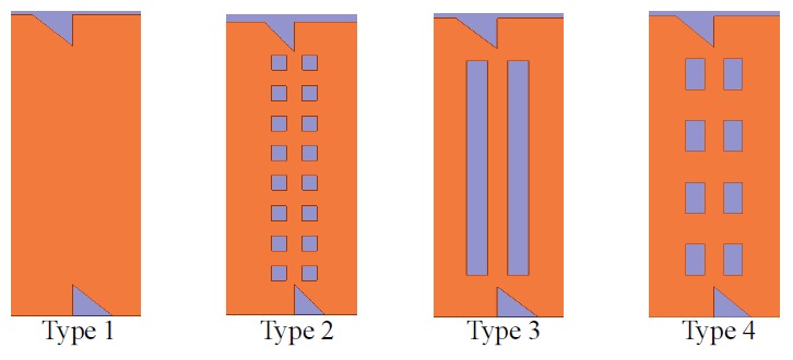
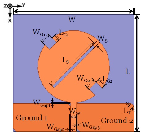
Fig. 3 shows the structure of the wideband patch antenna to radiate the CP. A coplanar waveguide (CPW) fed circular disc monopole with linear polarization for ultra-wideband (UWB) application has been proposed [9]. The antenna in [9] was composed of a radiating patch and a CPW feeder on a single layer-metallic structure. We have selected the antenna structure from [9] to realize the wide bandwidth and the CP radiation because that antenna had the wade bandwidth characteristics for UWB application and a circular disc patch with an easily modified structure for the CP radiation. In the present study, the thickness of the substrate and relative permittivity for the antenna design were 1.6 mm and 4.4 +
[Table 1.] The geometric parameters of the antenna (Fig. 3)

The geometric parameters of the antenna (Fig. 3)
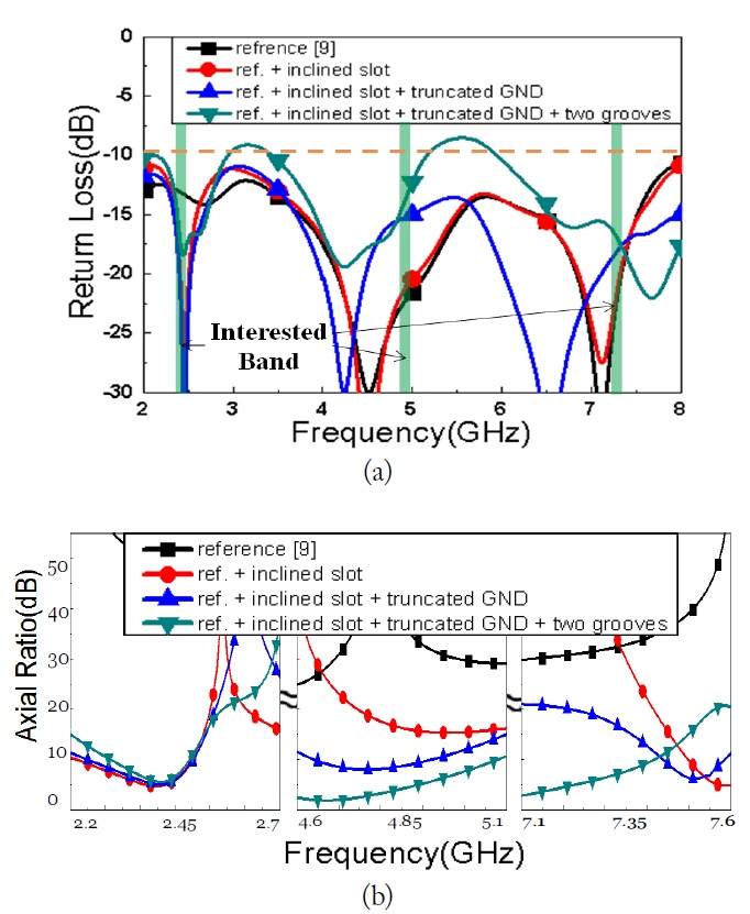
Fig. 4 shows the simulation results for the reference antenna [9] and the modified antenna shown in Fig. 3. The reference antenna with the linear polarization had been studied for the UWB application with the wide bandwidth. The CP design was the structure that included a truncated corner of the ground plane, a 45° inclined slot, two rectangular grooves on the circular disc patch and the CPW feeding structure with an asymmetric gap (
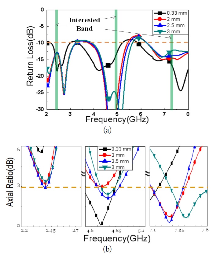
A good axial ratio was realized by varying the gap of
Fig. 6 shows the operating principle of the axial ratio change realized by the various gap distances. It supports the validity of the simulation results analyzed in Fig. 5.
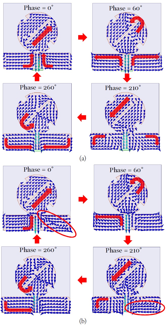
Fig. 6(a) and (b) show the electric currents distributions for a symmetric gap and an asymmetric gap, respectively, based on the antenna structure of Fig. 3 at transmitting band (2.44 GHz). In the case of the symmetric gap shown in Fig. 6(a), when the phase equals to 60° and 260° in Fig. 6(a), the surface currents on radiating patch and ground 2 plane flow in opposite directions to each other. This disturbs the radiation of the CP. On the other hand, when the phase is equal to 0° and 210°, as marked by a circle in Fig. 6(b), the flow of the surface currents on ground 2 plane with the asymmetric gap changes to compare with the current direction in Fig. 6(a). This current phase difference appears to depend on the asymmetric gap distance and influences the improvement in axial ratio. The asymmetric gap from Fig. 5 is considered in the remainder of this paper.
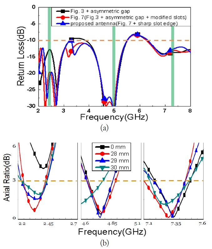
Even though the axial ratio was improved by asymmetric gap control, as shown in Fig. 6(b), it is still not 3 dB lower at the transmitting band. In order to solve the problem of the axial ratio improvement at the transmitting band, the modified 45° inclined slots were considered in the simulation design, as shown in Fig. 7. Table 2 indicates the simulated parameters of the modified slots in Fig. 7. The
However, the good axial ratios are still shifted from the center frequency of each band. In order to solve this problem, the edge configuration of the rectangular slots shown in Fig. 7 changes the tapering sharp slot edge shape.
[Table 2.] The simulated modification slot parameters in Fig. 7

The simulated modification slot parameters in Fig. 7
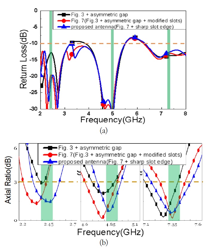
The effect of varying the slot edge shape on the return loss and the axial ratio was studied by conducting a simulation of tapering sharp slot edge shape, as shown in Fig. 9. The simulated return loss shown in Fig. 9(a) was essentially unchanged by variation in the modified slots and the sharp slot edge shape. On the other hand, the axial ratio shown in Fig. 9(b) showed a slight dependence on the shape of the slot edge. A reasonable axial ratio for the proposed antenna, expressed blue line with triangle symbols, was obtained at each center frequency of the triple bands. It was conformed that the slot edge shape can be control the frequency shift.
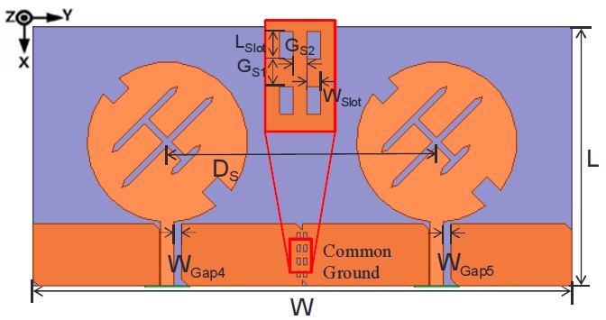
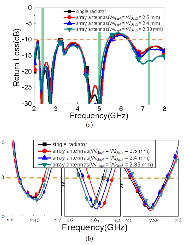
The performance of the proposed antenna was investigated in linear array environments. A linear array composed of two elements was considered, in order to assess the behavior of the individual elements in the array environment. A common ground for the linear array was also proposed to reduce the array dimension size and to increase the antenna gain. Many slots lie between the common ground as shown in Fig. 10. They blocked the field directly coupled from one element to its neighbors [11]. This novel technique allows reduction in the mutual coupling without increasing the distance between the elements.
The dimensions of the array antennas are shown in Table 3. The mutual coupling can be controlled by the slot number, slot shape, slot size and slot array structure. Even though the common ground plane with trapezoidal slot array looks like a connection, it actually operates as a separate single element by slots located on the common ground plane [11]. Therefore, the slot array design on the common ground plane is important.
[Table 3.] The geometric parameters of the linear array antennas shown in Fig. 10

The geometric parameters of the linear array antennas shown in Fig. 10
Fig. 11 shows three configurations with and without slots on the common ground plane, which is placed between two antenna elements.
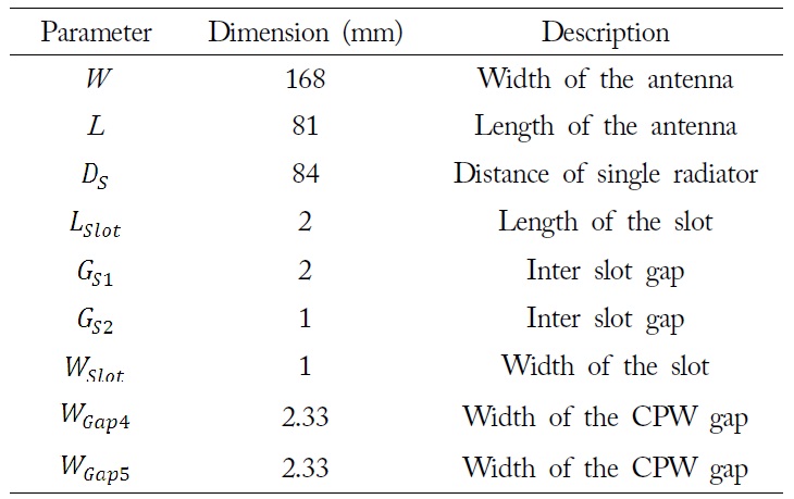
The effect of the shape, the size and the number of slots on the characteristics of the proposed antenna was investigated by simulating the linear array structure with four types of common ground plane, as shown in Fig. 12. The simulated return loss shown in Fig. 12(a) was essentially unchanged, which meant that the mutual coupling between two radiators was very weak and independent. However, the axial ratios of 2nd band and 3rd band strongly depended on the shape of the slot, as shown in Fig. 12(b), even though the axial ratio of the transmitting band was slightly changed.
Type 4 in Fig. 11 shows an excellent axial ratio. The good axial ratio for the 2nd band was shifted about 70 MHz. This was due to the gap distance of
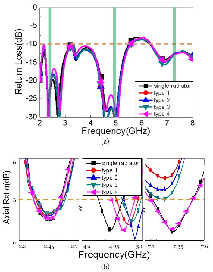
Fig. 13 shows the simulated results as functions of gap distance variation of
Fig. 14 shows the simulated results as functions of variation of
Furthermore, the axial ratio strongly depended on the distance of
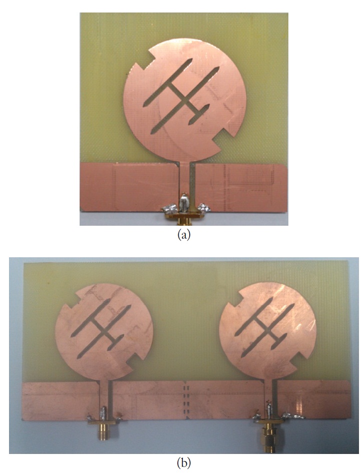
In order to verify the propriety of two proposed antennas, the novel antennas with CP were fabricated as shown in Fig. 15.
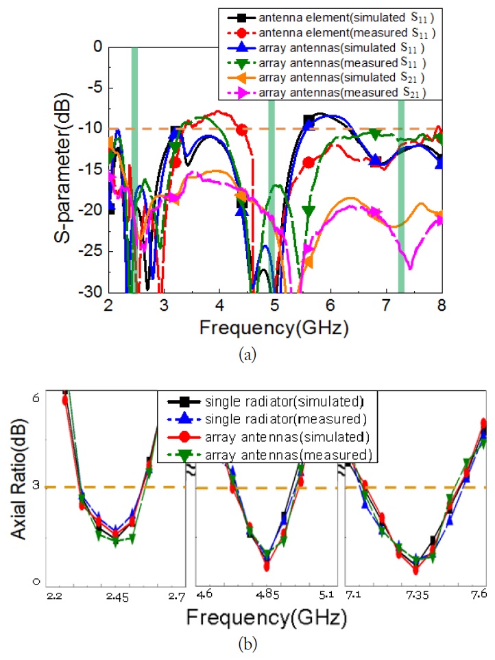
Fig. 16(a) indicates a comparison of the simulated and measured S-parameter. The bands of interest show reasonable agreements with enough bandwidth.
Simulated and measured isolation was also -20 dB lower at the all bands of interest. The axial ratio as shown in Fig. 16(b) was measured and compared. It shows very fine agreement with predicted values.
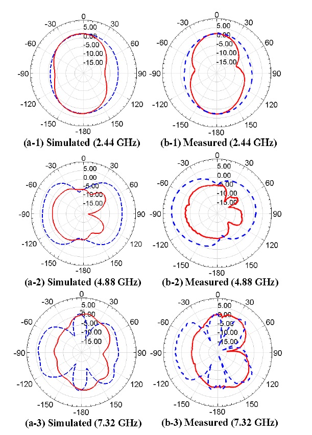
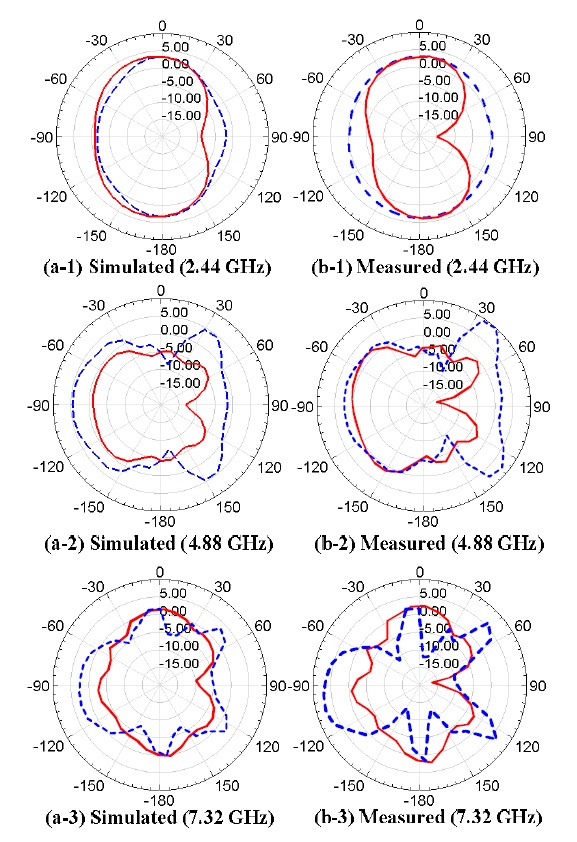
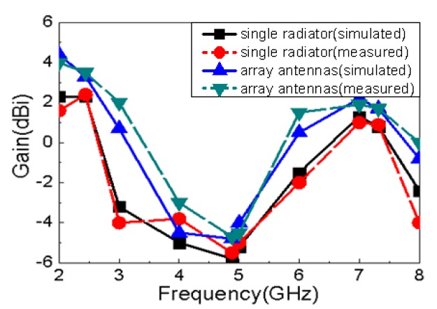
Figs. 17 and 18 show the simulated and measured gain directivity patterns at the each center frequency of the bands of interest. The measured patterns showed reasonable agreement with the simulated patterns. The simulated gains of array antenna are 3.3, 4.8, and 1.7 dBi at 2.44, 4.88, and 7.32 GHz, respectively. The measured and the simulated gain directivity patterns agreed with those of the single radiator.
Fig. 19 shows the gain comparison between the single radiator and array antennas from 2 to 8 GHz, where at θ = 0° and Ø = 0°. The gain of the array antennas was about 1 dBi higher than the gain of a single radiator.
This paper presents a theoretical analysis of small hidden device detection and a design for a triple band CP patch array antenna that uses the NLJD system. The axial ratio of a disc radiator was improved by including an asymmetric gap and an inclined slot modification. The axial ratio of the single radiator was also improved by truncating the corner at the ground edge. A good axial ratio that was 1.5 dB lower at the bands of interest was realized by the modified slot length and the asymmetric gap distance obtained from current distribution control on the radiating and ground planes. Improvement in the gain of a single radiator was achieved with linear array antennas with common ground plane. The common ground plane includes the optimum trapezoidal slot array to reduce mutual coupling without increasing the distance between the radiators. A higher gain is realized by using the novel common ground structure. The measured return loss was ?12 dB lower at the bands of interest. The simulated return loss and the axial ratio of the proposed antenna agreed well with the measured results. The measured E-field gain patterns of the x?z plane as well as the y?z plane are also showed very good agreement with the simulated results.

![Comparison of the simulation results between the reference
antenna [9] and the modified antenna shown in
Fig. 3. (a) The return loss and (b) axial ratio.](http://oak.go.kr/repository/journal/12792/E1ELAT_2013_v13n4_214_f004.jpg)