The semiconductor industry has made an approximate 30% reduction in production cost during the last decade, through the shrinkage of device size, introduction of new material, and improved yield management [1]. 300 mm sized wafer manufacturing industries have already adopted advanced process control (APC) with real-time process monitoring technique, to reduce equipment wait time waste (WTW) and process cost waste (PCW), which is represented as a normalized difference between instantaneous throughput and averaged throughput over a period of time [2].
PECVD process is a workhorse for dielectric thin film deposition of various materials, but during the deposition process, the chambers become coated with process chemicals. To maintain deposition process performance, the chambers are periodically cleaned with
Generally speaking, the chamber cleaning time and amount of gas usage varies, depending on the type of material and the amount of deposited layer in previous processes. Real-time monitoring of chamber cleaning with added sensors has been investigated, to improve productivity, waste reduction and cost reduction. One can expect to prevent failure by cross-contamination from imperfect chamber cleaning. Fourier transform infrared (FTIR) was used to optimize the type and usage of cleaning gases in CVD for manufacturing cost reduction [4], and multi-sensor study on reducing PFC gas emission in CVD chamber cleaning has been performed employing quadrupole mass spectrometry (QMS) [5]. FTIR and QMS can provide benefits of monitoring chamber residual gases from exhaust, but they require additional set up for real-time data acquisition.
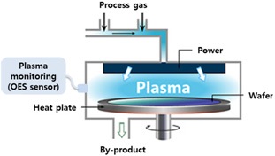
Optical emission spectroscopy (OES) is a reliable, in-situ and non-invasive monitoring method in plasma processing, and it is widely accepted as an end point detection (EPD) and process diagnosis in plasma etch [6-9]. In this paper, we practiced EPD of the PECVD chamber cleaning process, using OES. The targeted PECVD chamber for the cleaning process monitoring is the
Acquired real-time in-situ OES data was separated into two groups of process gases and by-product gases. Principal component analysis (PCA) was applied, to create a combined end point, tracing signals for the respective groups. Overlapping the two end point traces from the feeding gas group and byproduct group provided a straightforward intuition on the end point of PECVD chamber cleaning. Section II describes how the cleaning experiment was performed in the university research environment. EPD trace signal generation using PCA and its data analysis are presented in Section III. Finally, the conclusion is augmented with the Green Fab challenge in the research environment in Section IV.
Plasma enhanced chemical vapor deposition (PECVD) process requires a good amount of gas phase atoms or molecules to exist in the process chamber, and they are absorbed on the wafer surface to form a film. It is known that larger dissociation energy is required for
During the effort to develop a new process, in fact, we experienced a good amount of unabsorbed silicon by-product inside the chamber, in the form of powder and film on the chamber. The required time and effects for chamber cleaning were significant under the university research environment, thus in-situ chamber cleaning monitoring was an urgent technical issue to solve, for the reduction of equipment wait time waste (WTW), and equipment output waste (EOW).
The PECVD system used in this research was the PECVD MINIPLASMA-Station, manufactured by Plasmart Co. Ltd., Korea. The process chemistry for
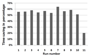
A total of eleven chamber cleaning runs were performed after every five
[Table 1.] Chamber cleaning process recipe.
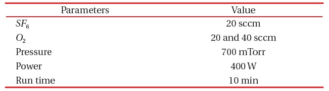
Chamber cleaning process recipe.
noticed a lesser amount of oxygen was enough for the chamber cleaning recipe. The first five cleaning runs were performed with 40 sccm of oxygen, and the rest were run with 20 sccm. This change does not affect the purpose of our experiment, which is the model building for end time trace data generation.
To ensure the quality of OES data to include the cleaning end point, we intentionally double the five minutes of cleaning time, which was previously set up. Sulfur hexafluoride (
While five cleaning runs were performed, 200 e five cleaning runs were performed, in Fig. 1. with monitoring, and locally stored for further data analysis. The OES system employed is a CCD type spectrometer, SM440 with Toshiba TCD 1304 sensor array, manufactured by Korea Spectral Product, and the data acquisition software was sensor cluster manager (SCM) from Prime Solutions. Once the data collection was made, the selection of corresponding peaks to plasma gas chemistry, decomposition of process gas and by-product gas, and modeling for end point trace signal generation were performed as shown below.
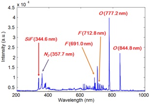
Selecting corresponding emission peak lines of the OES signal may be arduous, when the possible combinations of by-product are many. To alleviate this concern, principal component analysis (PCA) has been applied, to reduce the data dimensionality. However, separating reactant and by-product gas species by engineering intuitive can also be beneficial in our case. The deposited material on the chamber was mainly
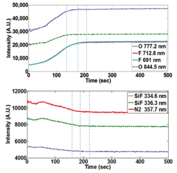
It is also straightforward that, as cleaning is performed, the optical emission intensity of feeding (or reactant) gases gradually increases, and that of by-products decreases, near the cleaning end point.
Figure 3(a) shows the reactant gases of fluorine and oxygen
trace signals, and Fig. 3(b) shows two peaks of
3. OES DATA ANALYSIS FOR CHAMBER CLEANING END POINT DETECTION
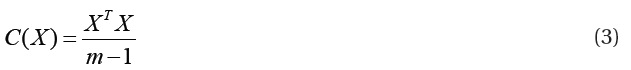
Principal component analysis (PCA) is an eigenvector-based multivariate analysis method that utilizes an orthogonal transformation, to reform the observation of interrelated variables towards the value of uncorrelated variables, called principal components (PCs) [11]. PCA has been widely used for multidimension data analysis, pattern recognition, and predictive regression models. PCA finds combinations of variables or factors that represent majority trends in a data set. PCs can be derived by an eigenvector decomposition of the covariance matrix of
[Table 2.] Covariance matrix of matrix X; (a) process gas and (b) byproduct gas.
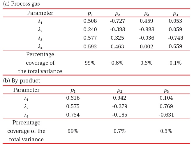
Covariance matrix of matrix X; (a) process gas and (b) byproduct gas.
where the data matrix

Here, n is the number of principal components, which must be less than or equal to the smaller dimension of

Here,
This assumes that the columns of

Raw data is normalized with the Z-score, with Z(0,1). The
quantity Z represents the distance between the raw score and the population mean, in units of the standard deviation. A covariance matrix is calculated from the Z-score data, and eigenvectors and eigenvalues of the covariance matrix are represented in Table 2.
Eigenvalues show their percentage of each
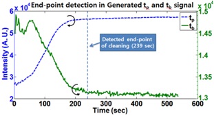
Figure 4 shows the newly generated
In this paper, we presented the usefulness of in-situ chamber cleaning monitoring and its end point detection in the PECVD process. Although in-situ optical emission spectroscopy (OES) data includes some data preprocessing for mathematical model building, the established model can efficiently detect the chamber cleaning end point. The result shows a cleaning time reduction of about 53% was achieved by employing the suggested chamber cleaning EPD, and this methodology can contribute to the semiconductor industry, by reducing wait time waste (WTW), and process cost waste (PCW).
The PECVD chamber cleaning process employs fluorinated gas, and over use of the cleaning agent should be minimized, to satisfy the Green Fab challenge. Although this fundamental research was performed at a laboratory level, it is desired to continuously expand it to semiconductor manufacturing facilities, by utilizing the currently available in-situ process monitoring technique.