The current trend towards smaller integrated electronic devices has strongly motivated intensive study on various nanostructures. Graphene possesses several unique electronic, mechanical, and optical properties, including high electron transport, high roomtemperature carrier mobility, high mechanical strength, and high optical transmittance. These properties, among others, make graphene an attractive candidate for applications including nanoelectronics, chemical and biochemical sensors, and transparent electrodes. Carbon-based materials, such as carbon nanotubes (CNTs) and graphene nanoribbons (GNRs), are being studied as interconnect materials, because they have lower resistivity [1-4], higher thermal conductivity, and intrinsically higher currentcarrying capacity than Cu. The widespread use of graphene in these applications depends on the development of grapheme synthesis techniques. Graphene layers have been fabricated using a variety of different methods, such as the mechanical exfoliation of graphite (i.e., the scotch tape method), high-temperature annealing of SiC, reduction of grapheme oxide, and chemical vapor deposition (CVD) method. Among the many studies on the synthesis of graphene, thermal decomposition method and chemical vapor deposition (CVD) are quite suitable for electronic applications due to the possibility of large-scale film growth [5-8]. CVD requires catalytic metal films such as Ni and Cu, and posttransfer techniques are required to support the graphene on a substrate. Therefore, it is desirable to control the strength of graphene- metal interactions to facilitate graphene characterization and processing [9,10]. Both theoretical and experimental studies have revealed that the chemical doping of graphene with foreign atoms such as nitrogen, boron, and sulfur can be used to define the electronic properties and chemical reactivity [11-13].
The characteristics of graphene doped by nitrogen atoms were investigated using graphene was grown by the thermal decomposition method. The physical properties of graphene film grown with various deposition conditions and doping times were investigated using Raman spectra.
The thermal decomposition method was used to deposit carbon and catalyst films onto SiO2/Si and Si substrates with an ambient annealing temperature of 1,000℃ during deposition for 30 min. Cu foil was cleaned using acetone and methane before the deposition. For graphene growth, a mixed gas comprising 10 sccm of H2 and 30 sccm of CH4 was used with a pressure of 1 Torr in a vacuum. To improve the quality of graphene, the graphene was exposed to H2 atmosphere for reduction at 300℃. To transfer the graphene from the copper foil to SiO2/Si substrate, the copper foil was exfoliated by dipping in an etchant after annealing at 85℃ on a hot plate and applying a PMMA coating on the as-deposited film. To transfer the graphene to the SiO2/Si substrate, the PMMA coating was removed in acetone solution for 30 min. To improve the chemical and electrical performance of the graphene, some specimens were doped by nitrogen atoms using nitric acid for various dipping times. The characteristics of the graphene were analyzed by Micro-Raman spectroscopy at the Jeonju Center of the Korea Basic Science Institute. The room-temperature Micro-Raman spectra were obtained using a 487.55-nm Ar-ion laser in the range of 1,000 to 3,000 cm-1 for 1 to 20 min. The laser power applied to the sample was about 1.011 mW.
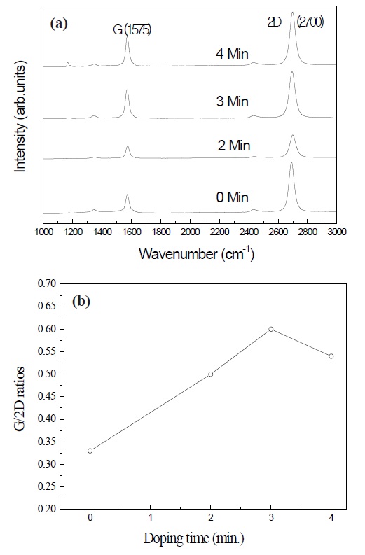
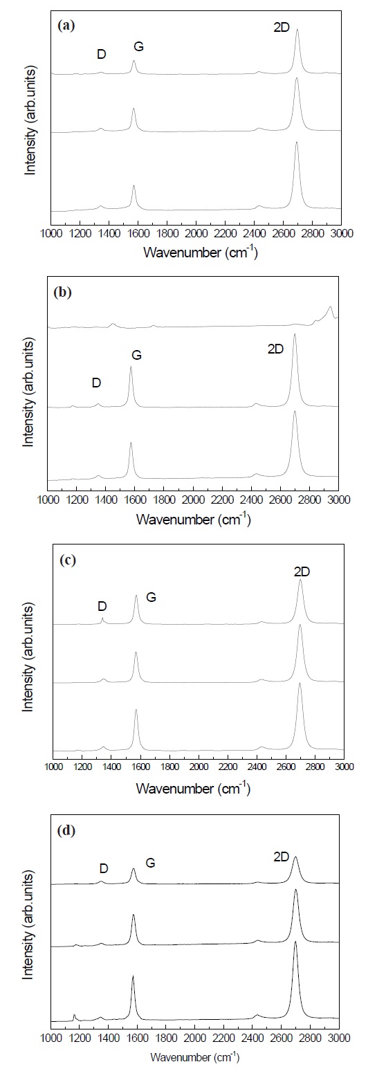
Figure 1 is the Raman spectra of graphene grown on copper foils with different doping time.
The D, G, and 2D peaks were observed at 1,350 cm-1, 1,757 cm-1, and 2,700 cm-1, respectively. The D peak at 1,350 cm-1 was very weak. All the samples showed a weaker G peak than the 2D peak. This result indicates that a few layers of graphene are grown on the SiO2/Si substrate. Graphene generally becomes monolayer graphene when the intensity of the G/2D ratio is weak.
Figure 2 shows the ratios of the G/2D intensity of graphene with various doping time. The graphene with the doping time of 3 min. had the highest intensity of G/2D. The electrical properties of graphene progress in the monolayer state. The effect of high doping with nitric acid makes the electrical properties degrade by the formation of graphene with multiple layers. Therefore, the results indicate that the doping time for monolayer graphene should be as short as possible for good performance.
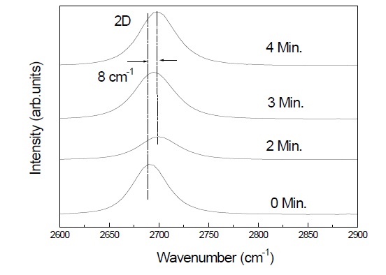
Figure 3 shows the Raman shifts of the 2D peak at about 2,700 cm-1 with respect to the doping of nitrogen atoms. Compared to the graphene without doping, the 2D peaks of the graphene doped with nitrogen shifted to a higher wave number by 8 cm-1.
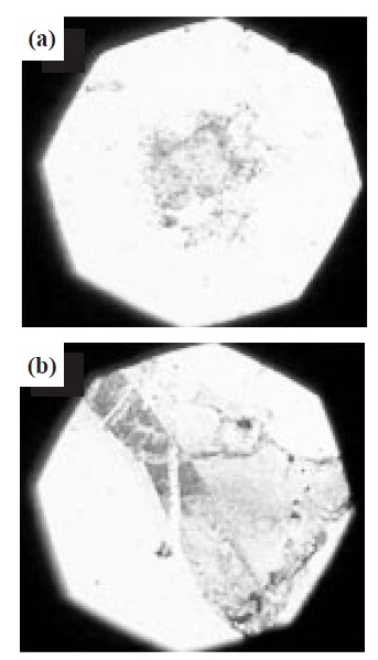
Figure 4 shows a surface image of graphene observed by optical microscopy. These images illustrate the polycrystalline nature of the graphene. Compared with the graphene prepared on SiO2, the graphene on the Si wafer exhibited multiple layers. Largearea graphene wafers are mostly grown on Cu foils, resulting in polycrystalline samples with a substantial number of grain boundaries, which are detrimental to the electronic properties [9]. The polarization of SiO2 supported the formation of monolayer graphene. The OH polarization at the interface between the Si surface and the graphene layers decreases the surface energy on the substrates for the graphene growth. Therefore, the SiO2 film was useful for the growth of monolayer graphene, as shown in Fig. 4(a).
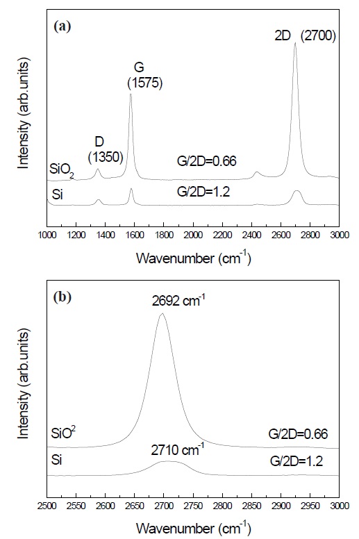
Figure 5(a) indicates the Raman shift of graphene prepared on SiO2 and Si wafers. The G/2D ratios of graphene made on SiO2 and Si were 0.66 and 1.2, respectively. The G/2D ratio is related to the graphene quality, in that the performance is better with lower G/2D ratios. Therefore, the results suggest that the graphene prepared
on SiO2 was improved compared to that grown on an Si wafer. Figure 5(b) shows the chemical shifts of the 2D peak at about 2,700 cm-1. The 2D peak of graphene prepared on Si wafer was shifted higher by about 8 cm-1 compared to that grown on SiO2. The chemical shifts may be attributed to the formation of multi-layers graphen. High-quality graphene was obtained in samples with low G/2D ratios, as shown in Figs. 3 and 5(b). The increase in the intensity of the G/2D ratios showed a blue shift in the 2D peaks.
Graphene was prepared on Cu foil by thermal chemical composition method with a gas mixture of H2 and CH4. The value of the D/2G intensity ratios defines the quality of the graphene, and monolayer graphene is indicated by a low D/2G ratio. The high quality of graphene showed a 2G peak at 2,692 cm-1. The monolayer graphene showed a red shift in the 2G peak near 2,692 cm-1. The increase in intensity of the G/2D ratios by the nitrogen doping was related to the multiple layers of graphene and the shift to a high wavenumber in the Raman spectra. The quality of graphene was affected by the nitrogen doping, and the G/2D ratio increased with the doping time. The graphene grown on SiO2 had a lower intensity of G/2D then that on Si wafer, because SiO2 acts as a buffer
between Si and graphene, and because of the polar properties of SiO2.